Electron Devices and Circuits: Unit I: PN Junction Devices
Unbiased P-N Junction
• In a given material if the doping is not uniform then at one place large number of charge carriers exist while at other place small number of charge carriers exist.
Unbiased P-N Junction
•
In a given material if the doping is not uniform then at one place large number
of charge carriers exist while at other place small number of charge carriers
exist. In a high charge carrier concentration area, all charge carriers are of
similar type, either electrons or holes and hence start repelling each other.
Due to this, charge carriers start moving from high concentration area towards
low concentration area, to achieve uniform concentration all over the material.
This process is called diffusion and exists when there is nonuniform
concentration of charge carriers in the material. In a p-n junction, on n side
there are large number of electrons while on p side electrons are minority in
number. So there is high concentration of electrons on n side while low
concentration of electrons on p side. Hence diffusion starts and electrons
start moving from n side towards p side.
•
Similarly the holes from p side diffuse across the junction into the n-region.
•
The initial diffusion is shown in the Fig. 1.4.1.
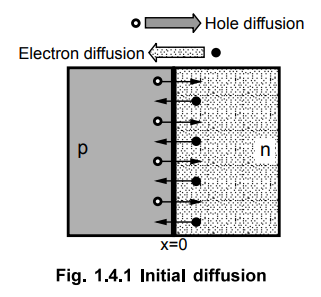
Fig. 1.4.1 Initial diffusion
1. Formation of Depletion Region
•
As holes enter the n-region, they find number of donor atoms. The holes
recombine with the donor atoms. As donor atoms accept additional holes, they
become positively charged immobile ions. This happens immediately when holes
cross the junction hence number of positively charged immobile ions get formed
near the junction on n side.
•
Atoms on p side are acceptor atoms. The electrons diffusing from n side to p
side recombine with the acceptor atoms on p side. As acceptor atoms accept
additional electrons, they become negatively charged immobile ions. Such large
number of negatively charged immobile ions get formed near the junction on p
side. The formation of immobile ions near the junction is shown in the Fig.
1.4.2.
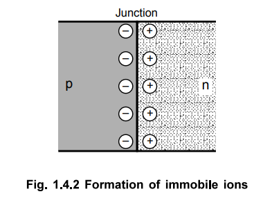
Fig.
1.4.2 Formation of immobile ions
•
As more number of holes diffuse on n side, large positive charge gets
accumulated on n side near the junction. Eventually the diffusing holes which
are positively charged, get repelled due to accumulated positive charge on n
side. And the diffusion of holes stops.
•
Similarly due to large negative charge accumulated on p side, the diffusing
electrons get repelled and eventually the diffusion of electrons also stops.
•
Thus in thermal equilibrium, in the region near the junction, there exists a
wall of negative immobile charges on p side and a wall of positive immobile
charges on n side. In this region, there are no mobile charge carriers. Such a
region is depleted of the free mobile charge carriers and hence called
depletion region or depletion layer. The depletion region is also called
space-charge region. In equilibrium condition, the depletion region gets
widened upto a point where no further electrons or holes can cross the
junction. Thus depletion region acts as the barrier.
•
The physical distance from one side to other side of the depletion region is
called width of the depletion region.
•
Practically width of the depletion region is very small of the order of few
microns where 1 micron = 1 × 10- 6 m.
2. Barrier Potential
•
Due to immobile positive charges on n side and negative charges on p side,
there exists an electric field across the junction. This creates potential
difference across the junction which is called barrier potential, junction
potential, built-in potential or cut-in voltage of p-n junction.
•
The barrier potential depends on,
1.
Type of semiconductor
2.
The donor impurity added
3.
The acceptor impurity added
4.
The temperature
5.
Intrinsic concentration
•
The barrier potential is called height of the depletion region and expressed in
volts. Symbolically it is denoted as VJ , Vo or Vr.
3. Effect of Doping on Depletion Region
•
The width of the depletion region depends on the amount of doping on n side and
p side. If the two sides are equally doped, the width of the depletion region
is equal on both sides as shown in Fig. 1.4.4 (a).
But if n side is heavily doped as compared to p side, then depletion region is observed more on p side as shown in the
Fig. 1.4.4 (b). If p side is heavily doped as compared to n side, then depletion region is observed more on n side as shown in the Fig. 1.4.4 (c).
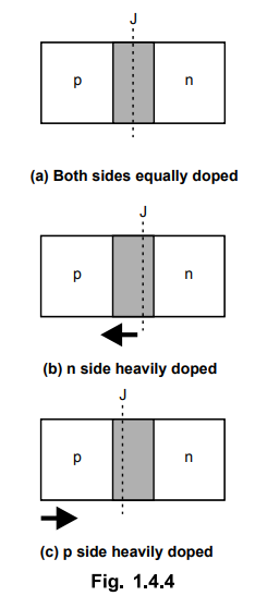
Key
Point : The depletion region penetrates more on the
lightly doped side.
Review Questions
1. Explain how a P-N junction is formed?
2. What is p-n junction? Explain the formation of depletion
region in unbiased p-n junction.
Electron Devices and Circuits: Unit I: PN Junction Devices : Tag: : - Unbiased P-N Junction
Related Topics
Related Subjects

Electron Devices and Circuits
EC3301 3rd Semester EEE Dept | 2021 Regulation | 3rd Semester EEE Dept 2021 Regulation