Linear Integrated Circuits: Unit IV: Special ICs
Voltage Controlled Oscillator Circuit (IC 566)
Operating working principle, Block Diagram, Pin Diagram, Functions of Pins, Symbol, Features, Functional diagram, Waveform, Circuit Diagram, Applications, Solved Example Problems
A voltage controlled oscillator is an oscillator circuit in which the frequency of oscillations can be controlled by an externally applied voltage. The VCO provides the linear relationship between the applied voltage and the oscillation frequency.
Voltage Controlled Oscillator Circuit (IC 566)
May-05,07,08,10,11,14,15,16,
Dec.-03,06,09,10,ll,15,16,17
A
voltage controlled oscillator is an oscillator circuit in which the frequency
of oscillations can be controlled by an externally applied voltage. The VCO
provides the linear relationship between the applied voltage and the
oscillation frequency. Applied voltage is called control voltage. The control
of frequency with the help of control voltage is also called voltage to
frequency conversion. Hence VCO is also called voltage to frequency converter.
Practically VCO is used to produce square and triangular waveforms whose frequency
is controlled by control voltage.
The
Fig. 4.2.1 shows op-amp based voltage controlled oscillator circuit.
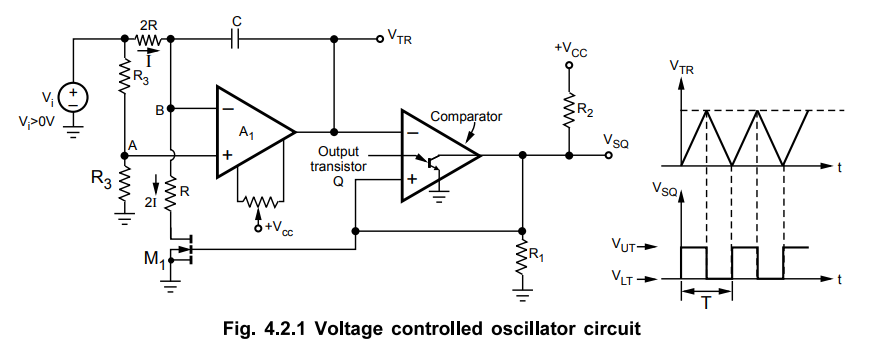
The
circuit associated with op-amp A1 is V-I converter i.e. it forces
current through capacitor C which is linearity proportional to the input
voltage Vi. For getting triangular and square waveforms, capacitor
must charge and discharge and thus current direction through capacitor must
keep on alternating. The direction of current through capacitor is controlled by
the MOSFET switch Mi. It is driven by Schmitt trigger comparator CMP. When the
output of CMP is low, M1 is off and resistance R remains floating
while when the output of CMP is high, M1 is on and resistance R gets connected
to the ground. The squarewave is obtained at terminal VSQ and
triangular wave is obtained at VTR. When output transistor Q is on,
VSQ is nothing but VCE(sat) i-e- almost zero. While when
Q is off then VSQ is decided by voltage divider of R1 and
R2.
VSQ
= VCC R1 / R1 + R2 .... when Q is off
As
the output VSQ is connected to the non inverting terminal of
comparator CMP, the high and low values of VSQ are the upper and
lower threshold levels of comparator CMP.
Due
to voltage divider of R3 and R3, the voltage of node A is,
VA
= Vi R3 / R3 R3 = Vi / 2 …. (4-2.1)
Due
to the virtual ground, VB = VA
VB
= Vi / 2 .... (4.2.2)
Thus
the current I through 2R resistor is,
The
equation (4.2.3) shows that op-amp A i acts as voltage to current converter.
Assume
that the output VSQ is low hence M1 is off and the
resistance R is floating.
So
entire current I = 4R(Vi) has to pass through the capacitor C and
the voltage VTR starts decreasing, due to polarity of voltage across capacitor.
So VTR ramps down.
When
VTR becomes zero then comparator CMP changes its state and output VSq
becomes high. Due to this M1 becomes on and the resistance R gets
connected to the ground. The current through resistance R is thus.
IR
= VB / R = Vi / 2R = 2 Vi / 4R = 2I …. (4.2.4)
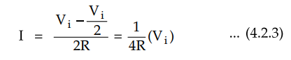
Now
current I out of 2I is supplied by resistance 2R but remaining current I must
be supplied by capacitor, as shown in the Fig. 4.2.2. Thus the direction of
current through the capacitor reverses. Hence VTR starts ramping up
i.e. starts increasing. It can be noted that capacitor current I gets
maintained at same magnitude only its direction gets reversed hence a
triangular waveform is available at VTR. As soon as VTR
reaches the level of VSQ, the schmitt trigger comparator changes its
state making M1 off. Thus the current I through capacitor again
reverses its direction and VTR ramps down. Thus the cycle continues.
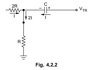
Period
of Oscillation
The
period of oscillation is determined by equating the charge expressions,
CΔV
= IΔt
During
any half cycle,
The
equation (4.2.5) shows that the output frequency is linearly proportional to
the input voltage Vi and thus circuit works as voltage controlled
oscillator.
But
the accuracy of such VCO circuit is limited because of speed of response of
op-amp A i comparator CMP and MOSFET switch M1. Similarly error is
caused at low frequencies due to input bias current and the offset voltage of
op-amp A x. The non-zero channel resistance of M1 when it is on i.e.
rds(on) is another factor causing an error. Hence in practice
integrated version of VCO is used.
Example
4.2.1 In the VCO circuit shown in the Fig. 4.2.1, the various
parameters are R = 10 kΩ, C = 1.25 nF, VUT = 10 V and VLT
= 0 V. If input is changed from 10 mV to 10 V calculate the range over which
the output frequency can be varied.
Solution
:
For the VCO circuit,
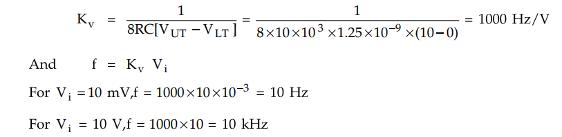
Hence
the range over which output frequency can be varied is 10 Hz to 10 kHz.
1. Voltage Controlled Oscillator (VCO) 1C 566
A
Voltage Controlled Oscillator (VCO) is an oscillator circuit in which the
frequency of oscillations can be controlled by an externally applied voltage.
The VCO provides the linear relationship between the applied voltage and the
oscillation frequency. Applied voltage is called control voltage. The control
of frequency with the help of control voltage is also called voltage to
frequency conversion. Hence VCO is also called voltage to frequency converter.
Practically VCO is used to produce square and triangular waveforms whose
frequency is controlled by control voltage.
Practically
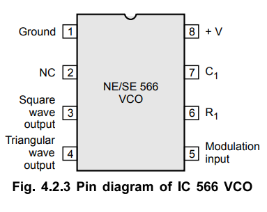
VCO is available in IC form. The commonly used VCO ICs are NE/SE 566, LM 566
etc. The Fig. 4.2.3 shows the pin diagram of NE/SE 566 VCO manufactured by
Signetics. It is 8 pin IC, which provides two output pins. Its feature is that
simultaneously IC provides square and triangular wave outputs which are the
functions of input voltage. The input voltage is also called modulating input
voltage.
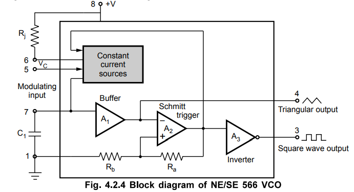
Operation
: The
op-amp A1 is used as a buffer. The op-amp A2 is used as a
Schmitt trigger and the op-amp A3 is used as an inverter. The
voltage VC is applied to the modulation input pin, which is a
control voltage.
The
capacitor C1 is linearly charged or discharged by a constant current
source. The charging current can be controlled by controlling the voltage VC at
pin 5 or by varying the resistance R1which is external to the IC.
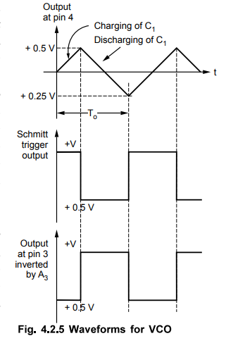
The charging and discharging levels are determined by the Schmitt trigger.
The
output voltage of Schmitt trigger is designed to swing between +V and 0.5 V.
For Ra = Rb, the voltage at noninverting terminal swings
between 0.5(+V) to 0.25(+V). Thus the triangular wave is generated due to
alternate charging and discharging of the capacitor C1, in linear
manner. When C1 voltage increases beyond 0.5(+V), the Schmitt
trigger output goes low, and the capacitor starts discharging. When the voltage
becomes less than 0.25 (+V), the output of the Schmitt trigger goes high. Due
to similar current sources used for charging and discharging, the time taken by
Ci to charge and discharge is same. This produces exact triangular wave. The
output of the Schmitt trigger output is step response which is available at the
pin 3 as a square wave output. The various waveforms are shown in the Fig.
4.2.5.
The
frequency of the output waveform is,
fo
= 2(+V – VC) / C1R1(+V) …. (4.2.7)
R1
should be in the range of 2 kΩ to 20 kΩ. The equation shows that the frequency
of the output oscillations is a frequency of the control voltage VC.
The frequency is also a function of the external resistance R1 and
capacitor C1.
2. Typical Connection Diagram of 566 VCO
Practically
the modulating input voltage at the pin 5 is controlled using a potential
divider formed by the resistances R2 and R3. Such a
circuit is shown in the Fig. 4.2.6.
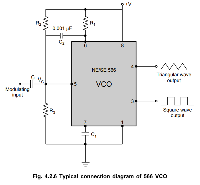
The R2 - R3 potential divider is used to set the control voltage VC. The initial voltage VC at the pins must be such that,
0.75(+V)
≤ VC <+V
where
+V is the supply voltage.
The
modulating input is connected through capacitor coupling to the pin 5 and it
must be less than 3V(p-p). For a fixed VC and Ci the frequency can
be varied in the range 10 : 1 by varying R1 between 2 kΩ to 20 kQΩ. For fixed R1
and C1 the frequency can be varied in the range 10 : 1 by varying control
voltage Vc. In both the cases maximum possible output frequency is 1 MHz. The
capacitor C2 connected between pins 5 and 6 is used to elliminate
any oscillations present in constant current source.
3. Features of 566 VCO
1.
Wide supply voltage range 10 V to 24 V.
2.
Very linear modulation characteristics.
3.
High temperature stability.
4.
Excellent power supply rejection.
5.
10 to 1 frequency range with fixed C1.
6.
The frequency can be controlled by means of current, voltage, resistor, or
capacitor
4. Derivation of Voltage to Frequency Conversion Factor
The
voltage to frequency conversion factor is an important factor of IC of 566. It
is denoted as Kv, and defined as,
Kv
= Δ fo / ΔVC ...
(4.2.8)
Here
Δ VC is the change in control voltage producing corresponding change
of Δ fo in the frequency.
fo
= New frequency
fo
= Original frequency ... (4.2.9)
Δ
fo = fo - fo
While
VC is changed by Δ VC to achieve this,
From
the expression of fo,
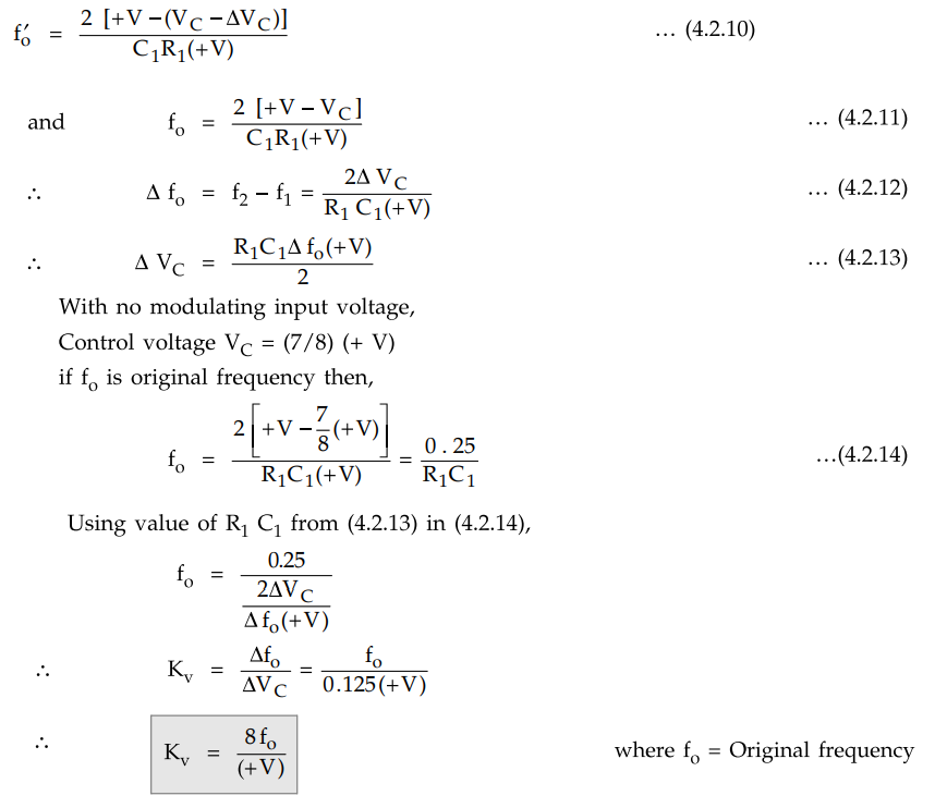
This
is the required voltage to frequency conversion factor.
Thus
output frequency can be expressed as,
fo
= Kv (+V) / 8
5. Applications of VCO
The
various applications of VCO are
1.
FM modulation.
2.
Signal generation (Triangular or square wave)
3.
Function generation.
4.
Frequency shift keying i.e. FSK demodulator.
5.
In frequency multipliers.
6.
Converting low frequency signals such as EEG and EKG into audio frequency range
signals.
7.
Tone generation.
6. Ramp Generator using 566
The
Fig. 4.2.7 shows the ramp generator using LM 566. Here, transistor Q1 is
used as short circuit path for capacitor. During charging the output at pin 3
is low (square wave). This makes Q1 OFF and hence capacitor charging
time is decided by the R 1r C1, +V and V C . When capacitor voltage charges
upto the upper threshold voltage of the Schmitt trigger, its output goes high,
making output at pin 3 high. As a result transistor Q1 is made ON.
It provides short circuit path for capacitor to discharge in no time. When
capacitor voltage goes below lower threshold of schmitt trigger, the voltage at
pin is made low, making transistor Q1 OFF. The capacitor Ci starts
charging again and cycle repeats.
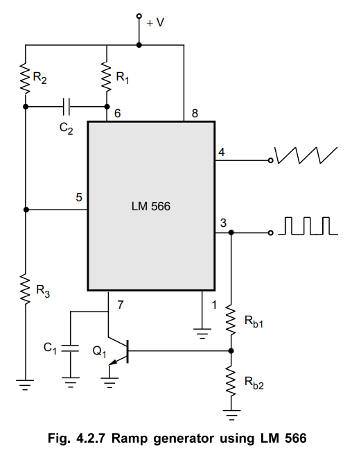
For
this circuit, capacitor charging time is decided by R1 C1,
+V and VC and discharge time is nearly zero. Therefore we get ramp
signal at the triangular wave output of the LM 566.
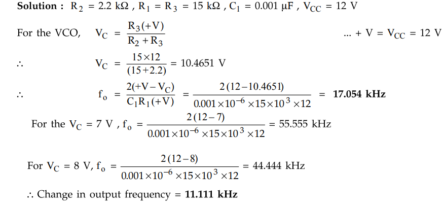
Example
4.2.1 For the VCO circuit, assume R2 -2.2 kQ,, R1 = R3 =
15 kQ, and C1 = 0.001 pF. Assume Vcc = 12 V. Determine the output frequency,
the change in output frequency if modulating input Vc is varied from 7 V to 8
V.
Dec.-14,
Marks 8
Solution
:
Review Questions
1. Explain the working
of voltage controlled oscillator.
2. Explain the voltage
controlled oscillator IC with a neat block diagram. Give its typical connection
diagram and its output waveforms.
3. With the help of
schematic circuit explain the operation of 566 voltage controlled oscillator.
State the expression for the output frequency. Discuss any two applications.
Dec.-06, 09,16,
May.-08, 10, 11, 14, 16, Marks 16
4. Define the voltage
to frequency converting factor and derive its expression. List the applications
of VCO.
May-03,05,06,07,12,
Dec.-03,04,08,10,16
Linear Integrated Circuits: Unit IV: Special ICs : Tag: : Operating working principle, Block Diagram, Pin Diagram, Functions of Pins, Symbol, Features, Functional diagram, Waveform, Circuit Diagram, Applications, Solved Example Problems - Voltage Controlled Oscillator Circuit (IC 566)
Related Topics
Related Subjects

Linear Integrated Circuits
EE3402 Lic Operational Amplifiers 4th Semester EEE Dept | 2021 Regulation | 4th Semester EEE Dept 2021 Regulation