Electron Devices and Circuits: Unit I: PN Junction Devices
Zener Diode
Symbols, Circuit Diagram, Operation principle, Characteristics, Equivalent Circuit, Breakdown Mechanisms, Comparison, Specifications, Applications
The zener diodes have breakdown voltage range from 3 V to 200 V. In 1934, a physicist Carl Zener investigated the breakdown phenomenon in the p-n junction diode.
Zener Diode
•
The zener diode is a silicon p-n junction semiconductor device, which is
generally operated in its reverse breakdown region. The zener diodes are
fabricated with precise breakdown voltages, by controlling the doping level
during manufacturing. The zener diodes have breakdown voltage range from 3 V to
200 V. In 1934, a physicist Carl Zener investigated the breakdown phenomenon in
the p-n junction diode.
•
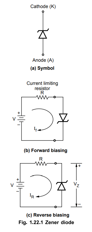
The Fig. 1.22.1 (a) shows the symbol of zener diode. The d.c. voltage can be
applied to the zener diode so as to make it forward biased or reverse biased.
This is shown in the Fig. 1.22.1 (b) and (c). Practically zener diodes are
operated in reverse biased mode.
1. Characteristics of Zoner Diode
•
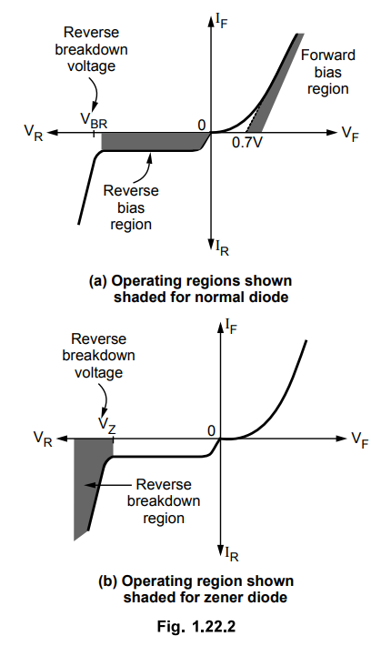
In the forward biased condition, the normal rectifier diode and the zener diode
operate in similar fashion. But the zener diode is designed to be operated in
the reverse biased condition. In reverse biased condition, the diode carries
reverse saturation current till the reverse voltage applied is less than the
reverse breakdown voltage. When the reverse voltage exceeds reverse breakdown
voltage, the current through it changes drastically but the voltage across it remains
almost constant. Such a breakdown region is a normal operating region for a
zener diode. The normal operating regions for a rectifier diode and a zener
diode are shown in the Fig. 1.22.2 (a) and (b).
•
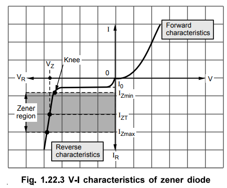
The breakdown characteristic for a zener diode is significantly important, as
it is an operating region for the diode. When the reverse voltage applied to a
zener diode is increased, initially the current through it is very small, of
the order of few µ.A or less. This is the reverse leakage current of the diode,
denoted by I0. At a certain reverse voltage, current through zener
diode increases rapidly. The change from a low value to large value of current
is very sharp and well defined. Such a sharp change in the reverse characteristics
is called knee or zener knee of the curve. At this knee, a breakdown is said to
occur in the device. The reverse bias voltage at which the breakdown occurs is
called zener breakdown voltage, denoted as Vz.
•
The voltage Vz is set by carefully controlling the doping level
during manufacturing process.
•
The current corresponding to a knee point is called zener knee current and it
is a minimum current zener must carry to operate in reverse breakdown region.
It is denoted as IZK or IZmin-
•
From the bottom of the knee, the zener breakdown voltage remains almost
constant, though it increases slightly as the zener current Iz, increases. The
current at which the nominal zener breakdown voltage is specified is called
zener test current, denoted as IZT. This value and corresponding
zener voltage VZ are specified on a datasheet of a zener diode.
Every zener diode has a capacity. As current increases, the power dissipation PZ
= VZ IZ increases. If this dissipation increases beyond
certain value, the diode may get damaged.
•
The maximum current a zener diode can carry safely is called zener maximum
current and is denoted as IZM or IZmax.
•
In practical circuits to limit the zener current between IZmin and IZmax, a
current limiting resistor is used in series with the zener diode.
•
The complete V-I characteristics of the zener diode is shown in the Fig.
1.22.3.
2. Equivalent Circuit of Zener Diode
•
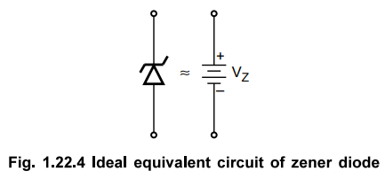
When the breakdown occurs then Iz may increase from IZmin to IZmax but voltage
across zener remains constant. Hence actually the internal zener impedance
decreases as current increases in the zener region. But this impedance is very
small. Hence ideally the zener diode is indicated by a battery of voltage Vz,
which remains fairly constant in the zener region. This is shown in the Fig.
1.22.4.
•
Practically though very small, zener has its internal resistance. In the zener
region, this resistance is called dynamic resistance of the zener denoted as
Zz. Practically zener region is not exactly vertical. The small change in zener
current ΔIZ produces a small change in zener voltage ΔVZ. The ratio of ΔVZ to ΔIz
is called zener resistance Zz. This is shown in the Fig. 1.22.5 (a). Hence
practically zener equivalent circuit is shown with a battery of Vz along with a
series resistance Zz as indicated in the Fig. 1.22.5 (b).
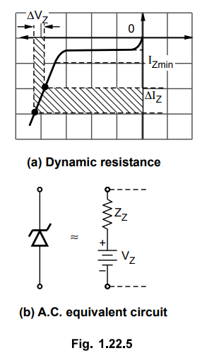
•
From the graph the dynamic resistance is defined as,
This
value is specified generally at zener test current IZT
Key
Point : In most of the cases this value is almost
constant over the full range of zener region i.e. from IZmin to Zmax' or<^er of few tens of ohms.
3. Breakdown Mechanisms in Zener Diode
•
There are two distinct mechanisms due to which breakdown may occur in the zener
diode. One is called zener breakdown and the other avalanche breakdown. For
most of commercially available silicon diodes, the maximum value of voltage
breakdown by the zener mechanism is low, in the region of 5 V to 8 V.
Consequently, for devices with breakdown voltages lower than 5 V, the zener mechanism
predominates, between 5 and 8 V, both zener and avalanche mechanism are
involved; whereas, above 8 V the avalanche mechanism alone takes over.
•
Practically zener breakdown is observed in the zener diodes with breakdown
voltages less than 6 V while avalanche breakdown is observed in the zener
diodes with breakdown voltages greater than 6 V. Commercially all such diodes
are referred as zener diodes whether breakdown mechanism is zener or avalanche.
a.
Zener Breakdown
•
The zener breakdown mechanism can be described qualitatively as follows :
The
application of reverse bias, voltage (6 V or less) causes a field across the
depletion region, at p-n junction, of the order of 3 × 10⁵ V/cm. An
electric field of such high magnitude exerts a large force on the valence
electrons of the atom, tending to separate them from their respective nuclei.
Actual breaking of the covalent bonds occurs when the electric field intensity
becomes more than 3 x 10⁵ V/cm. Hence, electron-hole pairs are generated in
large numbers and a sudden increase of current is observed. If a limiting
resistance in the circuit does not prevent the current from increasing to high
value, the diode may be destroyed because of excessive heating at the junction.
In zener breakdown, the value of breakdown voltage decreases as p-n junction
temperature increases, thus such diodes have negative temperature coefficient.
b.
Avalanche Breakdown
•
As seen earlier, the applied reverse bias causes a small reverse current I0
to flow in the device. This is due to movement of minority charge particles,
viz. electrons from the p-material and holes from the n-material. The polarity
of reverse bias voltage is such that only the minority charge particles are
able to cross the p-n junction, while the majority charge particles move away
from the junction. As the applied reverse bias voltage becomes larger, the
minority charge carriers increasingly accelerate. There are collisions between
these particles and electrons involved in the covalent bonds of the crystal
structure.
•
If the applied voltage is such that the travelling electrons do not have high
velocity, then the collisions take some energy away from them, altering their
velocity. If the applied voltage is increased, the velocity and hence the
kinetic energy (K. E. = 1/2 mv2 ) of electron increases. If such an electron
dashes against an electron involved in covalent bond, then the collision gives
bond-valence electron enough energy to enable it to break its covalent bond.
Thus, one electron by collision creates an electron-hole pair. These secondary
particles are also accelerated and participate in collisions that generate new
electron-hole pairs.
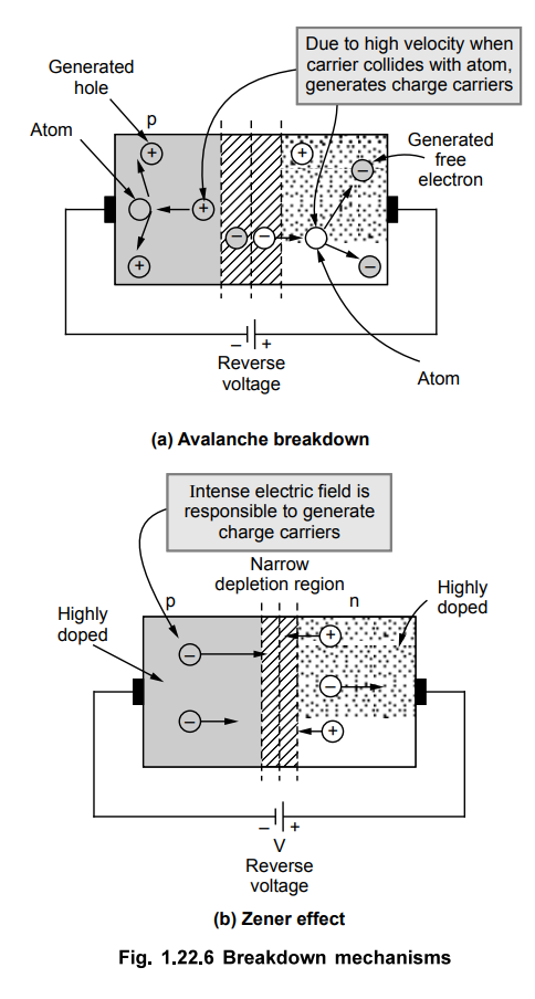
This
phenomenon is known as carrier multiplication. Electron-hole pairs are
generated so quickly and in such large number that there is an apparent
avalanche or self-sustained multiplication process. At this stage junction is
said to be in breakdown and current starts increasing rapidly. To limit such
current below IZmax, current limiting resistor is necessary.
•
Zener diodes having zener voltage above 6 V exhibit avalanche breakdown and
such diodes have positive temperature coefficient. The value of breakdown
voltage increases as p-n junction temperature increases. Thus zener diode has
positive temperature coefficient.
c.
Comparison of Breakdown Mechanisms
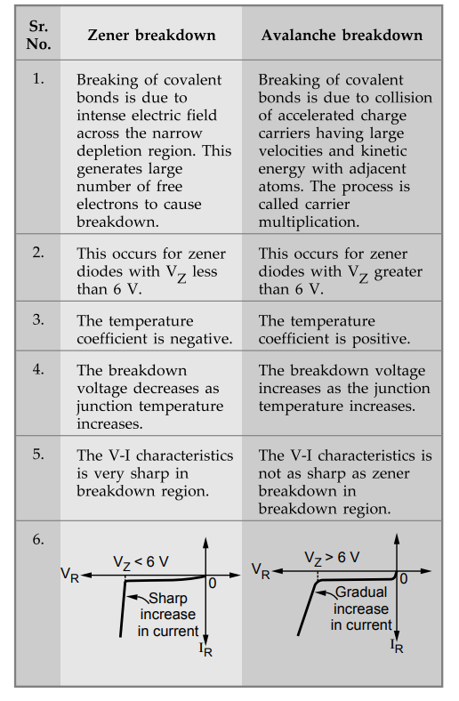
Zener
breakdown
1. Breaking of covalent bonds is due to
intense electric field across the narrow depletion region. This generates large
number of free electrons to cause breakdown.
2.
This occurs for zener diodes with Vz less than 6 V.
3.
The temperature coefficient is negative.
4.
The breakdown voltage decreases as junction temperature increases.
5.
The V-I characteristics is very sharp in breakdown region.
Avalanche
breakdown
1.
Breaking of covalent bonds is due to collision of accelerated charge carriers
having large velocities and kinetic energy with adjacent atoms. The process is
called carrier multiplication.
2.
This occurs for zener diodes with Vz greater than 6 V.
3.
The temperature coefficient is positive.
4.
The breakdown voltage increases as the junction temperature increases.
5.
The V-I characteristics is not as sharp as zener breakdown in breakdown region.
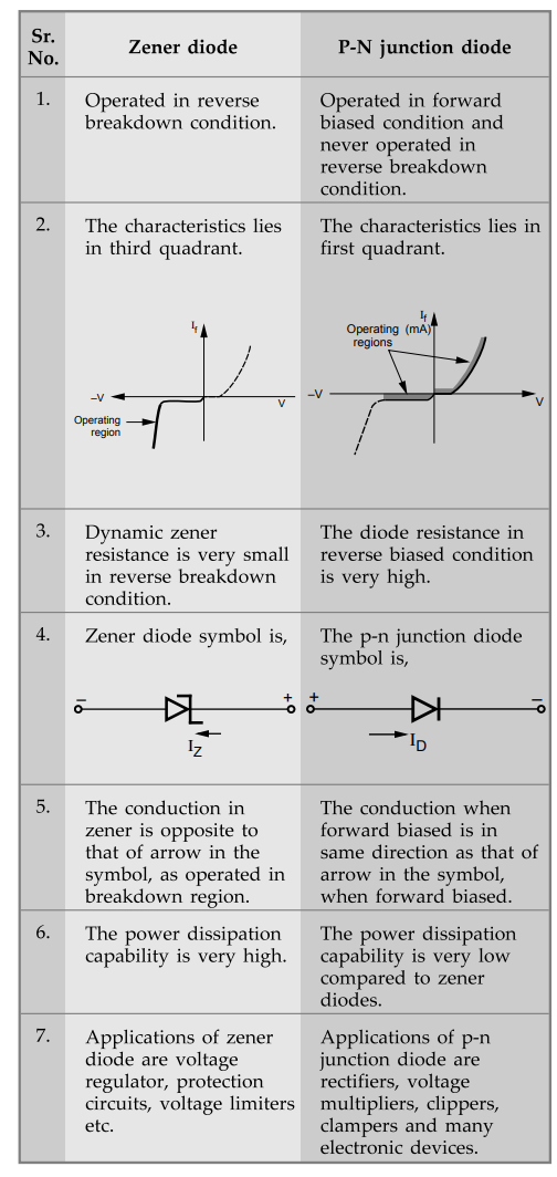
4. Comparison of Zener Diode and P-N Junction Diode
5. Specifications of Zener Diode
•
In the data sheet of zener diode, the important specifications or ratings about
a zener diode are specified. The various important specifications of a zener
diode are,
1.
Nominal Zener Voltage Vz or VZT : It is the voltage
across a zener diode when it is operated in its zener region. It remains
constant as long as zener diode is operated in the zener region. It is
specified at a specific value of zener test current denoted as I7T and has a
standard tolerance of ±10%
2.
Zener Test Current IZT : It is the reverse
current through a zener diode at which the nominal zener voltage Vz is specified.
At
this current various other parameters such as dynamic zener impedance are
specified.
3.
Dynamic Zener Impedance Zz or ZZT : This is a.c. zener
impedance which is the ratio of A VZ to AIZ. It is the reciprocal of the slope
of the zener characteristics in the zener region.
This
is generally specified at zener test current IZT. Some manufacturers
specify this at the zener knee current IZK or IZmin, hence denoted
as ZZK.
4.
Maximum Zener Current IZmax : The maximum reverse
current which a zener diode can carry safely without damaging it due to
excessive heating is called maximum zener current.
It
indicates the end of the zener region.
It
decides the maximum power dissipation rating of a zener diode.
5.
Minimum Zener Current IZmin or IZK :
The minimum reverse current which must flow through a zener diode to operate it
in the reverse biased condition is called minimum zener current.
It
is nothing but a current corresponding to a knee point. It is also called
breakover current or knee current.
It
indicates the start of a zener region.
6.
Maximum Power Dissipation PD(max) : It
is defined as the product of the zener voltage VZ and maximum zener
current IZmax
PD(max)
= VZ
× IZmax
•
The power dissipation in the zener diode must be less than PD(max)
to avoid the damage of the zener diode.
6. Applications of Zener Diode
•
The various applications of zener diode are,
1.
As a voltage regulating element in voltage regulators.
2.
In various protection circuits.
3.
In zener limiters i.e. clipping circuits which are used to clipp off the
unwanted portion of the voltage waveform.
Review Questions
1. Narrate the operation of a zener diode.
AU : May-08, Marks 6; Dec.-13, Marks 4
2. Explain V-I characteristics of zener diode.
AU : May-08, 10, Marks 8; Dec.-13, Marks 4
3. Draw and explain the V-I characteristics of a zener diode.
What are the two breakdown mechanisms in a zener diode ?
4. Differentiate between zener avalanche breakdown.
5. Compare zener diode and conventional p-n junction diode.
Electron Devices and Circuits: Unit I: PN Junction Devices : Tag: : Symbols, Circuit Diagram, Operation principle, Characteristics, Equivalent Circuit, Breakdown Mechanisms, Comparison, Specifications, Applications - Zener Diode
Related Topics
Related Subjects

Electron Devices and Circuits
EC3301 3rd Semester EEE Dept | 2021 Regulation | 3rd Semester EEE Dept 2021 Regulation