Microprocessors and Microcontrollers: Unit I: (c) 8085 Timing Diagrams
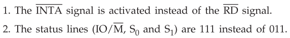
8085 Machine Cycles and their Timings
Opcode Fetch - Memory Read - Memory Write - I/O Read -I/O Write - Interrupt Acknowledge - Bus Idle
Questions : 1. Draw the timing diagram for I/O read operation and explain. 2. Draw and explain the timing diagram of opcode fetch machine cycle.3. Explain the interrupt acknowledge cycle for CALL instruction. 4. Draw and explain the bus idle machine cycle. 5. Draw and explain the timing diagram of memory write operation.
8085 Machine Cycles and their Timings
AU
: May-04,11,12,16, Dec.-05,10,12,15,16, June-12
The
8085 has seven machine cycles. These are :
1.
Opcode Fetch
2.
Memory Read
3.
Memory Write
4.
I/O Read
5.
I/O Write
6.
Interrupt Acknowledge
7.
Bus Idle
1. Opcode Fetch Cycle
The
first machine cycle of every instruction is opcode fetch cycle in which the
8085 finds the nature of the instruction to be executed. In this machine cycle,
processor places the contents of the Program Counter on the address lines and
through the read process, reads the opcode of the instruction. Fig. 5.4.1 (a)
shows flow of data (opcode) from memory to the microprocessor and Fig. 5.4.1
(b) shows the timing diagram for opcode fetch machine cycle. The length of this
cycle is not fixed. It varies from 4T-states to 6T-states as per the instruction.
The following section describes the opcode fetch cycle in step by step manner.

Step
1 : (State T1) In T1-state, the 8085
places the contents of program counter on the address bus. The high-order byte
of the PC is placed on the A8-A15 lines. The low-order
byte of the PC is placed on the AD0 - AD7 lines which
stays on only during T1. Thus microprocessor activates ALE (Address
Latch Enable) which is used to latch the low-order byte of the address in
external latch before it disappears.
In T1 8085 also sends status
signals 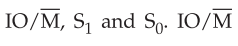 specifies whether it is a memory or I/O operation, S1
status specifies whether it is read/write operation; S1 and S0
together indicate read, write, opcode fetch, machine cycle operation or whether
it is in HALT state. In opcode fetch machine cycle status signals are
specifies whether it is a memory or I/O operation, S1
status specifies whether it is read/write operation; S1 and S0
together indicate read, write, opcode fetch, machine cycle operation or whether
it is in HALT state. In opcode fetch machine cycle status signals are 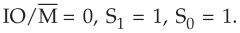
Step
2 : (State T2) In T2, low-order
address disappears from the AD0 - AD7 lines. (However A0
- A7 remain available as they were latched during T1. In
T2, 8085 sends![]() signal low to enable the addressed memory
location. The memory device then places the contents of addressed memory
location on the data bus (AD0 - AD7).
signal low to enable the addressed memory
location. The memory device then places the contents of addressed memory
location on the data bus (AD0 - AD7).
Step
3 : (State T3) During T3, 8085 loads the data from the
data bus in its Instruction Register and raises ![]() to high which
disables the memory device.
to high which
disables the memory device.
Step
4 : (State T4) In T4, microprocessor
decodes the opcode and on the basis of the instruction received, it decides
whether to enter state T5 or to enter state T1 of the
next machine cycle. One byte instructions those operate on eight bit data
(8-bit operand) are executed in T4.
For
example : MOV A, B, ANA D, ADD B, INR L, DCR C, RAL and many more.
Note
For one byte instructions which operate on eight bit data, data is always
available in the internal memory of 8085 i.e. registers.
Step
5 : (States T5 and T6) States T5
and T6, when entered, are used for internal microprocessor
operations required by the instruction. During T5 and T6, 8085 performs stack
write, internal 16-bit, and conditional return operations depending upon the
type of instruction. One byte instructions those operate on sixteen bit data
(16-bit operand) are executed in T5 and T6. For example :
DCX H, PCHL, SPHL, INX H etc.
2. Memory Read Cycle
The
8085 executes the memory read cycle to read the contents of R/W memory or ROM.
The length of this machine cycle is 3T-states (T4 - T3).
In this machine cycle, processor places the address on the address lines from
the stack pointer, general purpose register pair or program counter and through
the read process, reads the data from the addressed memory location. Fig. 5.4.2
(a) shows flow of data from memory to the microprocessor and Fig. 5.4.2 (b)
shows the timing diagram for memory read machine cycle. Memory read machine
cycle is similar to the opcode fetch machine cycle. However, they use only
states T4 to T3 and the status signal values 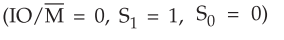 appropriate for
memory read machine cycle are issued in T1. The following section
describes the memory read machine cycle in step by step manner.
appropriate for
memory read machine cycle are issued in T1. The following section
describes the memory read machine cycle in step by step manner.

Step
1 : (State T1) In T1-state,
microprocessor places the address on the address lines from stack pointer,
general purpose register pair or program counter and activates ALE signal in
order to latch low-order byte of address.
During
T1 8085 sends status signals : 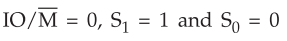 for memory read machine
cycle.
for memory read machine
cycle.
Step
2 : (State T2) In T2, 8085 sends ![]() signal low to enable the addressed memory location. The memory device
then places the contents of addressed memory location on the data bus (AD0
- AD7).
signal low to enable the addressed memory location. The memory device
then places the contents of addressed memory location on the data bus (AD0
- AD7).
Step
3 : (State T3) During T3, 8085 loads
the data from the data bus into specified register (F, A, B, C, D, E, H and L)
and raises ![]() to high which disables the memory device.
to high which disables the memory device.
3. Memory Write Cycle
The 8085 executes the memory write cycle to store the data into data memory or stack memory. The length of this machine cycle is 3T-states (T1 – T3). In this machine cycle, processor places the address on the address lines from the stack pointer or general purpose register pair and through the write process, stores the data into the addressed memory location. Fig. 5.4.3 shows the timing diagram for memory write machine cycle.

The memory write timing
diagram is similar to the memory read timing diagram, except that instead of  signal goes low during T2 and T3. The status signals for
memory write cycle are :
signal goes low during T2 and T3. The status signals for
memory write cycle are : 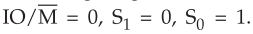 . The following section describes the
memory write machine cycle in step by step manner.
. The following section describes the
memory write machine cycle in step by step manner.
Step
1 : (State In T1) T1-state, the 8085 places the
address on the address lines from stack pointer or general purpose register
pair and activates ALE signal in order to latch low-order byte of address.
During T1 8085 sends status signals :
 for memory write machine cycle.
Step
2 : (State T2) In T2, 8085 places data
on the data bus and sends ![]() signal low for writing into the addressed
memory location.
signal low for writing into the addressed
memory location.
Step
3 : (State T3) During T3, ![]() signal goes high, which disables the memory device and terminates the write
operation.
signal goes high, which disables the memory device and terminates the write
operation.
4. I/O Read and I/O Write Cycles
The
I/O read and I/O write machine cycles are similar to the memory read and memory
write machine cycles, respectively, except that the  signal is high for
I/O read and I/O write machine cycles. High signal indicates that it is
an I/O operation. Fig. 5.4.4 (b) and Fig. 5.4.5 (b) shows the timing diagrams
for I/O read and I/O write cycles, respectively.
signal is high for
I/O read and I/O write machine cycles. High signal indicates that it is
an I/O operation. Fig. 5.4.4 (b) and Fig. 5.4.5 (b) shows the timing diagrams
for I/O read and I/O write cycles, respectively.


5. Interrupt Acknowledge Cycle
In
response to INTR signal, 8085 executes interrupt acknowledge machine cycle to
read an instruction from the external device. Theoretically, the external
device can place any instruction on the data bus in response to  .
However, only RST and CALL, save the PC contents (return address) before
transferring control to the interrupt service routine. The next sections
explain interrupt acknowledge cycles for RST and CALL instructions.
.
However, only RST and CALL, save the PC contents (return address) before
transferring control to the interrupt service routine. The next sections
explain interrupt acknowledge cycles for RST and CALL instructions.
Interrupt
acknowledge cycle for RST instruction
Fig.
5.4.6 shows the timing diagram of the interrupt acknowledge machine cycle and
execution of RST instruction. The interrupt acknowledge cycle is similar to the
opcode fetch cycle, with two exceptions.

During
interrupt acknowledge machine cycle (M1), the RST is decoded, which
initiates 1 byte CALL instruction to the specific vector location. The machine
cycles M2 and M3 are memory write cycles that store the
contents of the program counter on the stack and then a new instruction cycle
begins.
Interrupt
acknowledge cycle for CALL instruction
Fig.
5.4.7 shows the timing diagram of the interrupt acknowledge machine cycle and
execution of a CALL instruction. For CALL instruction, it is necessary to fetch
the two bytes of the CALL address through two additional interrupt acknowledge
machine cycles (M2 and M3 in the Fig. 5.4.7). The machine
cycles M4 and M5 are memory write cycles that store the
contents of the program counter on the stack and then a new instruction cycle
begins.
6. Bus Idle Cycle
These
are few situation where the machine cycles are neither Read nor Write. These
situations are :
1.
For execution of DAD instruction (this instruction adds the contents of a
specified register pair to the contents of HL register pair) ten T-states are
required. This means that after execution of opcode fetch machine cycle, DAD
instruction requires 6 extra T-states to add 16-bit contents of a specified
register pair to the contents of HL register pair. These extra T-states which
are divided into two machine cycles do not involve any memory or I/O operation.
These machine cycles are called BUS IDLE machine cycles. Fig. 5.4.8 shows Bus
Idle Machine Cycle for DAD instruction.

In
the case of DAD, these Bus Idle cycles are similar to memory read cycles,
except ![]() and ALE signals are not activated.
and ALE signals are not activated.
2.
During internal opcode generations, for TRAP and RST interrupts, 8085 executes
Bus Idle Machine Cycles. Fig. 5.4.9 shows the Bus Idle Machine Cycle for TRAP.
In response to TRAP interrupt, 8085 enters into a Bus Idle Machine Cycle during
which it invokes restart instruction, stores the contents of PC onto the stack
and places 0024H (Vector address of TRAP) onto the program counter.
The
number of machine cycles required to fetch complete instruction depends on the
instruction type :
1. One byte
2. Two byte or 3. Three byte.
One
byte instruction does not require any additional machine cycle. Two byte
instruction requires one additional memory read machine cycle, whereas three
byte instruction requires two additional memory read machine cycles.
The
number of machine cycles required to execute the instruction depends on the
particular instruction. The total number of machine cycles required varies from
one to five. It is possible that memory read and memory write machine cycles
occur more than once in a single instruction cycle. The following examples
illustrate the timing diagrams and machine cycles used for few 8085
instructions.
Example
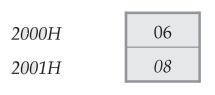
5.4.1 Draw the timing diagram for instruction MVI B, 08H
which is stored at address 2000H.
AU
: Dec.-10
Solution
: This
instruction consists of two bytes; the first is the opcode for MVI B
instruction and the second is the data byte. The 8085 needs to read these bytes
first from memory and thus requires at least two machine cycles. The first
machine cycle is opcode fetch and second is memory read. Fig. 5.4.10 shows the
timing diagram for this instruction. This instruction cycle is described in the
following paragraphs.

1. The first machine cycle is an opcode
fetch machine cycle. In T1 the microprocessor places the 16-bit
memory address (2000H) from the program counter on the address bus, 20H on the
A15-A8 and 00H on AD7 –AD0 and
increments program counter to 2001H to point to the next memory location. It
activates ALE signal (active high) to latch the low-order address OOH from the
bus AD7 –AD0 . It
also gives the status signals ( , S1 and S0) Oil
to indicate that it is an opcode fetch machine cycle. In T2, the 8085 activates
, S1 and S0) Oil
to indicate that it is an opcode fetch machine cycle. In T2, the 8085 activates ![]() (active low) and reads the contents of memory location 2000H i.e. 06H. Then
8085 places the opcode in the instruction register and disables the
(active low) and reads the contents of memory location 2000H i.e. 06H. Then
8085 places the opcode in the instruction register and disables the ![]() signal during T3. During T4, the 8085 decodes the opcode
and recognizes that it needs memory read machine cycle to read second byte of
the instruction. In T4, the contents of the bus A15 – A8
are unknown, and the data bus AD7 – AD0 goes into high
impedance state.
signal during T3. During T4, the 8085 decodes the opcode
and recognizes that it needs memory read machine cycle to read second byte of
the instruction. In T4, the contents of the bus A15 – A8
are unknown, and the data bus AD7 – AD0 goes into high
impedance state.
2. After opcode fetch machine cycle 8085
executes memory read machine cycle. In ?! of memory read machine cycle, 8085
places the address 2001H on the address bus and increments the program counter
to point the next memory location (2002H). 8085 then activates ALE signal and
sends status signals  010 to indicate memory read machine cycle. During
T2 and T3, 8085 activates
010 to indicate memory read machine cycle. During
T2 and T3, 8085 activates ![]() signal and reads the 8-bit
data from memory location 2001H (08H). The 8085 then stores this data into the
accumulator.
signal and reads the 8-bit
data from memory location 2001H (08H). The 8085 then stores this data into the
accumulator.
Example
5.4.2 Indicate machine cycles and T-states
required for execution of STA Instruction
AU
: May-16, Marks 8
Solution
:
For instruction shown in Fig. 5.4.11, three machine cycles are required to
fetch the instruction and one additional machine cycle is required to store the
contents of accumulator into the memory. So following machine cycles are
required for STA instruction.

1.
Opcode Fetch (4T- states). 2. Memory Read
(3T- states).
3.
Memory Read (3T- states). 4. Memory Write
(3T- states).
Thus
for STA instruction 13T-states are required.
Example
5.4.3 Indicate machine cycles and T-states required
for execution of LXI instruction.
Solution
: For
instruction shown in Fig. 5.4.12, three machine cycles are required to fetch
the instruction. As it is an immediate instruction, operand i.e. immediate
16-bit data is given within the instruction, no further machine cycle is required.

Machine
cycles required for LXI instruction.
1.
Opcode Fetch (4T- states). 2. Memory Read (3T- states).
3.
Memory Read (3T- states).
Thus
for LXI instruction lOT-states are required.
Example
5.4.4 Indicate machine cycles and T-states
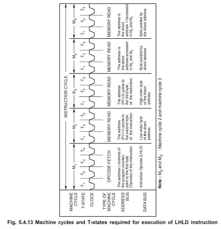
required for execution of LHLD instruction.
Solution
:
For instruction shown in Fig. 5.4.13 (See on next page), three machine cycles
are required to fetch the instruction and two additional machine cycles are
required to load 16-bit contents from two consecutive memory locations into HL
register pair. So following machine cycles are required for LHLD instruction.
1.
Opcode Fetch (4T-states). 2. Memory Read
(3T-states).
3.
Memory Read (3T-states). 4. Memory Read
(3T-states).
5.
Memory Read (3T-states).
Thus
for LHLD instruction 16T-states are required.
Review Questions
1. Draw the timing
diagram for I/O read operation and explain.
2. Draw and explain
the timing diagram of opcode fetch machine cycle.
3. Draw and explain
the timing diagram of memory read machine cycle.
4. Draw and explain
the timing diagram of memory write machine cycle.
5. Draw and explain
the timing diagrams for I/O read and I/O write machine cycles.
6. Explain the
interrupt acknowledge cycle for RST instruction.
7. Explain the
interrupt acknowledge cycle for CALL instruction.
8. Draw and explain
the bus idle machine cycle.
9. Indicate machine cycles and T-states required for execution of LDA instruction.
10. Explain the use of Ready signal in 8085.
11. Illustrate the
timing diagram for the execution of instruction MVI B, 08 in 8085.
AU: Dec.-10, Marks 10
12. Draw the timing
diagram of opcode fetch machine cycle and I/O read cycle.
AU: May-12, Marks 8
13. With timing
diagram, explain the memory read operation in 8085 microprocessor.
AU: May-11, Dec.-12,
Marks 4
14. Draw the timing
diagram for opcode fetch machine cycle and memory read machine cycle.
AU: Dec.-12, Marks 8
15. Draw and explain
the timing diagram of memory write operation.
AU: Dec.-14, Marks 8
16. Draw the timing
diagram of Opcode Fetch machine cycle.
AU: Dec.-15, Marks 8
17. Explain the timing
diagram of STA 526 AH
AU :May-16, Marks 8
18. Draw the timing
diagram for I/O read and Write Machine cycles.
AU: Dec.-16, Marks 8
Microprocessors and Microcontrollers: Unit I: (c) 8085 Timing Diagrams : Tag: : Opcode Fetch - Memory Read - Memory Write - I/O Read -I/O Write - Interrupt Acknowledge - Bus Idle - 8085 Machine Cycles and their Timings
Related Topics
Related Subjects
Microprocessor and Microcontroller
EE3404 MCU 4th Semester EEE Dept | 2021 Regulation | 4th Semester EEE Dept 2021 Regulation