Microprocessors and Microcontrollers: Unit IV: (e) Keyboard and Display Controller - 8279
Block Diagram
Keyboard and Display Controller - 8279
It consists of four main sections : • CPU interface and control section • Scan section • Keyboard section • Display section
Block Diagram
AU
: Dec.-09, 11, 12, 13,15, May-11, 13, 16
Fig.
12.5.1 shows the block diagram of 8279. It consists of four main sections :
•
CPU interface and control section
•
Scan section
•
Keyboard section
•
Display section
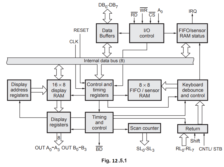
1. CPU Interface and Control Section
This
section consists of data buffers, I/O control, control and timing registers,
and timing and control logic.
Data
Buffers : The data buffers are 8-bit bi-directional buffers
that connect the internal data bus to the external data bus.
I/O
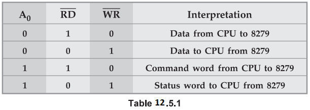
Control : The I/O control section uses the A0,  signals to control data flow to and from the various internal registers and
buffers. The data flow to and from the 8279 is enabled only when
signals to control data flow to and from the various internal registers and
buffers. The data flow to and from the 8279 is enabled only when ![]() = 0;
otherwise the 8279 signals are in a high impedance state. The 8279 interprets
the data given or desired by the CPU with the help of A0,
= 0;
otherwise the 8279 signals are in a high impedance state. The 8279 interprets
the data given or desired by the CPU with the help of A0,  signals, as shown in Table 12.5.1. When Ao is logic 0 data is transferred and
when Ao is logic 1 command word or status word is transferred. determine
the direction of data flow through the data buffers.
signals, as shown in Table 12.5.1. When Ao is logic 0 data is transferred and
when Ao is logic 1 command word or status word is transferred. determine
the direction of data flow through the data buffers.
Control
and Timing Registers : The control and timing registers
store the keyboard and display modes and other operating conditions programmed
by the CPU. The modes are programmed by sending the proper command on the data
lines with A0 = 1. The command is latched on the rising edge of ![]() .
The command is then decoded and the appropriate mode/function is set.
.
The command is then decoded and the appropriate mode/function is set.
Timing
Control : The timing control consists of the basic timing
counter chain. The first counter is divided by N prescaler that can be
programmed to give an internal frequency of 100 kHz. The prescalar can take a
value from 2 to 31.
2. Scan Section (Scan Counter)
The
scan section has a scan counter which has two modes : Encoded mode and Decoded
mode.
Encoded
mode : In the encoded mode, the scan counter provides a
binary count from 0000 to 1111 on the four scan lines (SC3 -SC0) with active
high outputs. This binary count must be externally decoded to provide 16 scan
lines.
Display
can use all 16 scan lines to interface 16 digit 7-segment display, but keyboard
can use only 8 scan lines out of 16 scan lines.
Decoded
mode : In the decoded mode, the internal decoder decodes
the least significant 2 bits of binary count and provides four possible
combinations on the scan lines (SC3 -SC0) : 1110, 1101,
1011 and 0111. Thus the output of decoded scan is active low. These four active
low output lines can be used directly to interface 4 digit 7 segment display, 8
× 4 matrix keyboard, eliminating the external decoder.
3. Keyboard Section
This
section consists of return buffers, keyboard debounce and control, FIFO/sensor
RAM and FIFO/sensor RAM status. There functions depend on selected keyboard
mode out of three keyboard input modes : scanned keyboard, sensor matrix and
strobed input.
Return
buffers : The 8 return lines (RL7 –RL0)
are buffered and latched by the return buffers during each row scan in scanned
keyboard or sensor matrix mode. In strobed input mode, the contents of the
return lines are transferred to the FIFO RAM on the rising edge of the CNTL/STB
line pulse.
Keyboard
debounce and control : Keyboard and debounce control is
enabled only when scanned keyboard mode is selected. In the scanned keyboard
mode, return lines are scanned, looking for key closures in that row. If the
debounce circuit detects a close switch, it waits about 10 msec to check if the
switch remains closed. If it does, the address of the switch in the matrix plus
the status of SHIFT and CONTROL keys are transferred to the FIFO RAM.
FIFO/Sensor
RAM : This is a dual function 8 × 8 RAM. In scanned
keyboard and strobed input modes, it is a FIFO. Each new entry is written into
successive RAM positions and then read in order of entry. In sensor matrix
mode, the memory is referred to as sensor RAM. Each row of the sensor RAM is
loaded with the status of the corresponding row of sensor in the sensor matrix.
FIFO/sensor
RAM status : FIFO RAM status keeps track of the
number of characters in the FIFO and whether it is full or empty. The status
logic also makes IRQ signal high when the FIFO is not empty, which can be used
to interrupt CPU telling that key press is detected and keycode is available in
FIFO RAM.
4. Display Section
The
display section consists of display RAM, display address registers and display
registers.
Display
RAM : It is 16 × 8 RAM, which stores the display codes
for 16 digits. It can be accessed directly by CPU. In decoded mode, 8279 uses
only first four locations of display RAM. In encoded mode, 8279 uses first
eight locations for 8 digit display and all 16 locations for 16 digits display.
Display
address registers : The display address registers hold the
address of the byte currently being written or read by the CPU and scan count
value. The read/write addresses are programmed by CPU command. If set in
autoincrement mode, address in the address register is incremented for each
read or write.
Display
registers : Display registers are two 4-bit
registers A and B. They hold the bit pattern of character to be displayed. The
contents of display registers A and B can be blanked and inhibited
individually.
Review Questions
1. Explain the
operation of the keyboard/display controller with a neat diagram.
AU : Dec.-09,11, Marks
8
2. What is the
function of scan section in 8279 programmable keyboard/display controller ?
AU : May-11, Marks 2
3. List the major
components of the 8279 keyboard / display interface and explain their functions
in detail.
AU : Dec.-12, Marks 8
4. Draw and explain
the architecture of 8279 keyboard / display controller.
AU : May-13, Dec.-13,
Marks 8
5. Explain the block
diagram, architecture and registers of the 8279 keyboard / display Controller.
AU : Dec.-15, Marks 16
6. With neat diagram,
explain the architecture and features of 8279 keyboard display controller.
AU : May-16, Dec.-17 Marks 16
Microprocessors and Microcontrollers: Unit IV: (e) Keyboard and Display Controller - 8279 : Tag: : Keyboard and Display Controller - 8279 - Block Diagram