Digital Logic Circuits: Unit I: (b) Digital Logic Families
Characteristics of Digital Logic Families
Classification, Performance
• The propagation delay of a gate is basically the time interval between the application of an input pulse and the occurrence of the resulting output pulse.
Characteristics of Digital Logic Families
AU
: Dec.-04, 05, 06, 08, Hay-05, 07, 08, 11, 14, 17
Propagation
Delay
•
The propagation delay of a gate is basically the time interval between the
application of an input pulse and the occurrence of the resulting output pulse.
The propagation delay is a very important characteristic of logic circuits
because it limits the speed at which they can operate. The shorter the
propagation delay, the higher the speed of the circuit and vice-versa. The
propagation delay is determined using two basic time intervals :
1.
tPLH : It is the delay time measured when output is changing from
logic 0 to logic 1 state (LOW to HIGH)
2.
tPHL : It is the delay time measured when output is changing from
logic 1 to logic 0 state (HIGH to LOW).
•
When tPHL and tPLH are not equal, the larger value is considered as
a propagation delay time for that logic gate, i.e.
tp
= max (tPLH' tPLH )
Power
Dissipation
•
The amount of power that an IC dissipates is determined by the average supply
current, ICC, that it draws from the VCC supply. It is the product of ICC and
VCC. For ICs, the value of ICC for a LOW gate output (ICCL) is
different from a HIGH output (ICCH)
•
Therefore, average ICC is determined based on the 50 % duty cycle operation of
the gate (LOW half of the time and HIGH half of the time).
ICC(avg)
= ICCH + ICCL / 2
•
This can be used to calculate average power dissipation as,
PD(avg)
= ICC(avg) × VCC
Current
and Voltage Parameter
VIH
(min) - High-Level Input Voltage : It is the minimum
voltage level required for a logical 1 at an input. Any voltage below this
level wall not be accepted as a HIGH by the logic circuit.

VIL(max)-
Low-Level Input Voltage : It is the maximum voltage level
required for a logic 0 at an input. Any voltage above this level will not be
accepted as a LOW by the logic circuit.
VOH
(min) - High-Level Output Voltage : It is the
minimum voltage level at a logic circuit output in the logical 1 state under defined
load conditions.
VOL
(max) - Low-Level Output Voltage : It is the maximum
voltage level at a logic circuit output in the logical 0 state under defined
load conditions.
IIH
- High-Level Input Current : It is the current that
flows into an input when a specified high-level voltage is applied to that
input.
IIL-
Low-Level Input Current : It is the current that flows into
an input when a specified low-level voltage is applied to that input.
IOH
- High-Level Output Current : It is the current that
flows from an output in the logical 1 state under specified load conditions.
IOL-
Low-Level Output Current : It is the current that flows from
an output in the logical 0 state under specified load conditions.
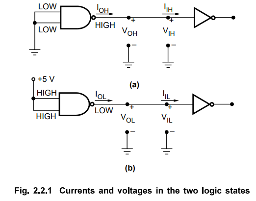
Note
:
The current directions shown in the Fig. 2.2.1 may be opposite to those
shown depending on the logic family.
Noise
Margin and Logic Voltages Levels
•
In digital circuits, the binary 0 and 1 are represented by a pair of voltage
levels. Each logic family has a different standard. The Table 2.2.1 shows the
voltages used by several families.

•
These are the ideal voltage levels. But in practice, it is difficult to get
these ideal voltages. Stray electric and magnetic field can induce voltages on
the connecting wires between logic circuits. These unwanted signals are called
noise and can sometimes cause the voltage at the input to a logic circuit to
drop below V„ or rise above ViL(max), which
could produce unpredictable operation. The noise immunity of at a logic circuit
refers to the circuit's ability to tolerate the noise without causing spurious
changes in the output voltage. To avoid this problem due to noise, voltage
level VIH(min) is kept at a few fraction of volts below VOH(min)
and VIL(max) VOL(max) design time. This is illustrated in
Fig. 2.2.2.
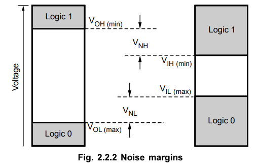
•
As shown in Fig. 2.2.2, VNH is the difference between the lowest possible HIGH
output, VOH(min) and the minimum voltage, VIH(min) required for a HIGH input.
This voltage difference, VNH is called high-state noise margin. Similarly, we
have low-state noise margin. It is the voltage difference between the largest
possible low output, VOL(max) and the maximum voltage, VIL(max) required for a
LOW input.
•
In short we can write as,
VNH
= VOH(min) _ VIH(min)
VNL
= VIL (max) - VOL(max)
•
The noise margin allows the digital circuit to function properly if noise
voltages are within the limits of VNH and VNL for a
particular logic family.
Fan-in
and Fan-out
•
In a digital system, we typically find many types of digital ICs interconnected
to perform various functions. In these situations, the output of a logic gate
may be connected to the inputs of several other similar gates. The maximum
number of inputs of several gates that can be driven by the output of a logic
gate is decided by the parameter called fan-out. In general, the fan-out is
defined as the maximum number of inputs of the same IC family that the gate can
drive maintaining its output levels within the specified limits. For example, a
logic gate with fan-out 10 can drive maximum 10 logic inputs from the same
family. It depends on current sourcing and sinking capacity of input and output
signals of same IC family.
•
The fan-in of a digital logic gate refers to the number of inputs. For example,
an inverter has a fan-in of 1, a 2-input NOR gate has a fan-in of 2, a 4-input
NAND gate has a fan-in of 4 and so on. A logic designer has to select the
fan-in of the gate to accommodate the number of inputs. At the hardware level,
however, the fan-in provides information about the intrinsic speed of the gate
itself. In general, the propagation delay increases with the fan-in. This means
that 2-input NAND gate is faster than the 4-input NAND if both are from same
logic family.
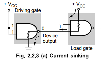
Current
Sinking
•
A device output is said to sink current when current flows from the power
supply, through the load and through the device output to ground. This is
illustrated in Fig. 2.2.3 (a).
Current
Sourcing
•
A device output is said to source current when current flows from the power
supply, out of the device output and through the load to ground. This is
illustrated in Fig. 2.2.3 (b).

Speed Power Product (Figure of Merit)
•
In general, for any digital IC, it is desirable to have shorter propagation
delays (higher speed) and lower values of power dissipation. There is usually a
trade-off between switching speed and power dissipation in the design of a
logic circuit i.e. speed is gained at the expense of increased power dissipation.
Therefore, a common means for measuring and comparing the overall performance
of an IC family is the Speed-Power Product (SPP). It is also called Figure of
Merit.
Review Questions
1. Define fan-in and fan-out.
AU : Dec.-08, 05, May-11, Marks 2
2. Differentiate : Source and sink current.
AU : May-07, Marks 2
3. Define power dissipation and propagation delay.
AU : May-05, Marks 2
4. Why does the propagation delay occur in logic
AU : Dec.-06, Marks 2
5. Define noise margin.
AU : Dec.-04, 08 May-07, 08, Marks 2
6. List the factors used for measuring the performance of
digital logic families.
AU : May-14, Marks 2
Digital Logic Circuits: Unit I: (b) Digital Logic Families : Tag: : Classification, Performance - Characteristics of Digital Logic Families
Related Topics
Related Subjects

Digital Logic Circuits
EE3302 3rd Semester EEE Dept | 2021 Regulation | 3rd Semester EEE Dept 2021 Regulation