Linear Integrated Circuits: Unit I: IC Fabrication
Crystal Growth and Water Preparation
IC Fabrication
The first important process in IC fabrication is the formation of a silicon wafer through the crystal growth. This process can be subdivided into number of sub processes as given below.
Crystal Growth and Water Preparation
The
first important process in IC fabrication is the formation of a silicon wafer
through the crystal growth. This process can be subdivided into number of sub
processes as given below.
1.
Silicon crystal ingots growing
2.
Ingot trimming and grinding
3.
Ingot slicing
4.
Wafer etching
5.
Wafer polishing
6.
Wafer cleaning
Let
us consider subprocess one by one.
1. Silicon Crystal Ingots Growing
The
important semiconductor material for the fabrication of semiconductor devices
and integrated circuits is silicon. Other semiconductor materials are germanium
and gallium arsenide. At present 95% of the semiconductor devices and integrated
circuits are manufactured using silicon only and for very special applications
gallium arsenide is preferred. We have already discussed that the bipolar
junction transistor (BJT) was developed first in 1948, with germanium as a
basic semiconductor material. But it was observed that silicon is better option
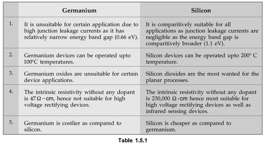
than germanium. The comparison between silicon and germanium is as given in
Table 1.5.1.
Basically
silicon is the element, found in nature in the form of silica and silicates. It
is found abundantly in the natrure in the form of silicon dioxide. So this
silicon dioxide constitutes almost 20 % of the earth's crust. So obviously one
can not start fabricating integrating circuits using silicon dioxide with the
earth's crust. The sand can be converted into pure silicon through number of
processes. For the fabrication of ICs, the silicon must be in crystalline form.
The crystalline form of silicon is the pure silicon with no deflects and no
contaminations.
To
obtain this purest form of silicon, first Metallurgical Grade Silicon (MGS) is
produced in a submerged electron arc furnace. Using this step, MGS is
solidified with a purity of about 98 %. Then the silicon is pulverized
mechanically. Then it is added with unhydrous hydrogen chloride to form
trichlorosilane (SiHCl3). This process is carried out with a catalyst in a
fluidized bed at 350 °C. After this reaction, the trichlorosilane obtained is
liquid at room temperature. Then by using fractional distillation, purification
of trichlorosilane is carried out. After this purified trichlorosilane is
applied with chemical vapour deposition process. With the help of chemical
reaction, hydrogen is reduced from trichlorosilane. It results in the rods of
silicon. This multistep process continues for many hours and finally results in
polycrystalline structured EGS rods with 0.2 m diameter and several meter
length. This process is advantageous because the costing of the process is low
and the byproducts of the reactions are less harmful. The Electronic Grade
Silicon (EGS) is also known as Semiconductor Grade Silicon (SGS) which the
highly purified form of silicon i.e. polycrystalline silicon. This form of
silicon consists many small crystals. However for fabrication of ICs a crystalline
silicon is needed. The single crystal silicon can be obtained by using method
known as crystal growth.
The
primary method of CCW the crystal growth
is Czochralski (CZ) method.
In
practice all the silicon required for integrated circuits is prepared by using
this method only. In general, a phase change from solid, liquid or gas phases
to crystalline solid phase is nothing but growing crystal. Czochralski method
is used for silicon crystal growth from which ultimately silicon wafers are
produced. The apparatus used for the crystal growth is called Czochralski
crystal growth apparatus or puller.
The
puller has four important subsystems namely
furnace, crystal pulling mechanism, ambient control and control systems. The
simplified Czochralski crystal puller is as shown in the Fig. 1.5.1
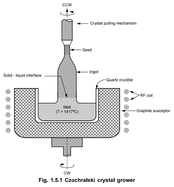
The
furnace consists a crucible, crucible support, rotation mechanism and heating
element housed in a chamber. The crucible is made up of fused silica (SiO2) as
this material is chemically unreactive with molten silicon. An EGS block is
heated in a fused silica crucible with the appropriate dopant using a heating
element. The material in the crucible is heated to a temperature which is
greater than the melting point of silicon, i.e. 1417°C. A resistance heating is
preferred for large pullers ; while induction heating is used for small melt
sizes.
Then
a small single crystal rod of silicon is immersed into the molten material.
This rod is called seed crystal. This seed crystal is located at the crystal
pulling assembly. In this assembly, using rotating mechanism seed shaft and
seed chuck are rotated. Lowering the seed crystal in molten silicon allows the
crystal ingot to form on the seed by solidification. The main function of
crystal pulling assembly, is to control the pull rate of seed crystal and
crystal rotation both, with minimum vibrations and precision. During the
crystal growth, the crystal is rotated slowly, by stirring the molten and
averaging out temperature gradients leading to inhomogeneous solidification. To
get the ingots of circular cross-section, the crucible and the seed crystal are
rotated in opposite direction. When the seed crystal is pulled out of the
molten material, due to solidification, silicon ingot gets formed exactly same
as seed crystal.
In
general, the diameter is controlled by the pull rate. The standard diameter of
the ingot is about 150 mm and the length is about 2 m. The ingot with such
dimensions weighs about 60 kg.
The
silicon growth is generally conducted in a vacuum or in an inert gas like helium
or argon.
To
control the process parameters such as temperature, crystal diameter, pull rate
and rotation speed etc, control system is used which works under either open
loop control or closed loop control.
2. Ingot Trimming and Grinding
First
of all, the seed which initiated the crystal growth is separated from the
circular ingot. The top and bottom ends are also cut off. As silicon is hard
and brittle material, industrial grade diamond is used for shaping and cutting
it. This process is called ingot trimming. After completion of the crystal
growth, it is generally tested for resistivity and perfection evaluation. So
the portions of the ingot failed in the above tests are also cut. Note that
these cuttings can be recycled for new crystal growth after cleaning.
After
trimming of the ingot, the surface grinding of the ingot is carried out.
Actually the ingots are slightly oversized. Hence with the help of lathelike
diamond tool, the ingot is ground to a precise diameter.
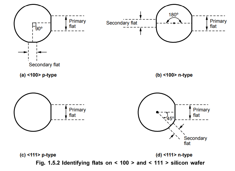
After
grinding the ingot to a precise diameter, generally two flats are ground along
the length of the ingot. The larger flat is called major or primary flat and it
is positioned relative to the crystal direction. The x-ray technique is used to
locate the primary flat. The primary flat is very important as
i)
it serves for mechanical alignment of the wafer in automatic processing, and
ii)
it serves for orienting ICs on the wafer relative to the crystal.
The
smaller flat is called secondary flat which is used to identify the orientation
(< 100 > or < 111 >) and conductivity (p or n) of the wafer.
3. Ingot Slicing
After
completing ingot trimming and grinding process, the ingot is ready for next
process i.e. ingot slicing. The slices of the ingot are called wafers and
typically the thickness of wafer may very from 0.4 mm to 1 mm. This process is
very important as it is necessary to maintain the flat plane and desired
surface orientations.
The
slicing also determines the orientation of the surface. In general, there are
two orientations < 100 > and < 111 >. Out of these orientations,
the wafers with < 100 > orientations are cut 'on orientation' ; while
wafers with < 111 > orientations are cut 'off orientations'. The position
of the flats can be identified according to the standards laid by the
Semiconductor Equipment and Materials Institute (SEMI) as shown in the Fig.
1.5.2.
 The
ingot is sliced using a circular cutting blade kept in tension on the outer
edge while having the cutting edge on the inner diameter.
The
ingot is sliced using a circular cutting blade kept in tension on the outer
edge while having the cutting edge on the inner diameter.
The
thickness of the wafer is determined by the slicing. It is another important
wafer parameter because thicker wafers can easily withstand the stresses of
subsequent thermal processes. The higher quality of slicing is achieved by
using capacitive sensing device near the blade which helps the blade to be
positioned correctly to achieve exactly flat plane cut.
4. Wafer Etching
If
the sliced wafers are to be used for VLSI application, then before etching
process two sided mechanical lapping process is carried out. Using this
process, wafers with uniform flatness are achieved which are mostly required
for photolithography.
Due
to the machining operations during trimming, grinding and slicing, the surface
and edges of the wafers get contaminated and even damaged. The depth of damage
depends on the mechanical operations carried previously. It is observed that
the damaged and contaminated regions are not more than 10 pm deep. Even by
using chemical etching process, all the damaged and contaminated edges can be
removed. Practically mixture of hydrofluoric, acetic and nitric acids is used
in chemical etching. This is called acidic etching. The other alternative is to
use alkaline etching using potassium hydroxide or sodium hydroxide. By the
etching process, typically 10 pm to 30 pm of wafer is removed from both the
sides.
5. Wafer Polishing
After
etching, the wafer is polished to eliminate the microcracks and debris. The
main intension of polishing a wafer is to provide a smooth and perfect flat
surface such that the device features can be engraved. The polishing is done
with the help of a polishing machine. Note that the polishing process removes
further 10 pm to 30 pm of the wafer surface typically.
The
three steps of lapping, etching and polishing reduce the wafer thickness by 40
to 150 pm. Thus by considering the typical figures, to have the wafer of 200 pm
thickness, the thickness of the substrate required is 560 pm. In practice, the
processed 6 inch wafers are typically 250 pm to 500 pm thick.
6. Wafer Cleaning
The
silicon wafers are cleaned using chemicals. Generally organic films, heavy
metals are deposited on the surface of the wafers. Hence by using HC1 - H2O2
aqueous solution, metallic impurities can be removed. First the wafer is
cleaned by using HCl - H2O2. Then wafer is rinsed in
water to deionize. Again the wafer is dipped in hydrofluoric acid. Then again
the wafer is rinsed in water.
After
cleaning process, the wafer is ready for the formation of the dies.
Review Questions
1. Describe the steps of crystal growth and water preparation in
detail.
2. Explain Czocharalski method of crystal growth with the help
of a neat diagram.
3. Write a note on ingot trimming and polishing.
4. Explain different orientations in silicon.
5. How is wafer etching carried out ?
Linear Integrated Circuits: Unit I: IC Fabrication : Tag: : IC Fabrication - Crystal Growth and Water Preparation
Related Topics
Related Subjects

Linear Integrated Circuits
EE3402 Lic Operational Amplifiers 4th Semester EEE Dept | 2021 Regulation | 4th Semester EEE Dept 2021 Regulation