Digital Logic Circuits: Unit III: (b) Analysis & Design of Synchronous Sequential Circuits
Design of Clock Sequential Circuits: State Assignment, Derivation of State
• In sequential circuits we know that the behaviour of the circuit is defined in terms of its inputs, present states, next states and outputs. To generate desired next state at particular present state and inputs, it is necessary to have specific flip-flop inputs.
2. State Assignment
•
In sequential circuits we know that the behaviour of the circuit is defined in
terms of its inputs, present states, next states and outputs. To generate
desired next state at particular present state and inputs, it is necessary to
have specific flip-flop inputs. These flip-flop inputs are described by a set
of Boolean functions called flip-flop input functions. To determine the
flip-flop input functions, it is necessary to represent states in the state
diagram using binary values instead of alphabets. This procedure is known as
state assignment. We must assign binary values to the states in such a way that
it is possible to implement flip-flop input functions using minimum logic
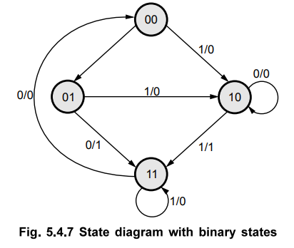
gates. Fig. 5.4.7 shows the state diagram shown in Fig. 5.4.2 after state
assignments.
Rules
for state assignments
•
There are two basic rules for making state assignments.
Rule
1 :
States having the same NEXT STATES for a given input condition should have
assignments which can be grouped into logically adjacent cells in a K-map.
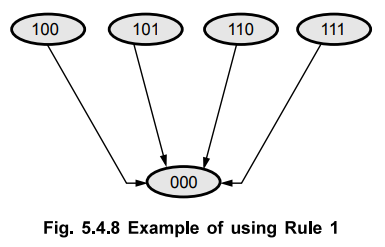
Fig. 5.4.8 shows the example for Rule 1. As
shown in the Fig. 5.4.8, there are four states whose next state is same. Thus
states assignments for these states are 100, 101,110 and 111 which can be
grouped into logically adjacent cells in a K-map.
Rule
2 :
States that are the NEXT STATES of a single state should have assignment which
can be grouped into logically adjacent cells in a K-map.
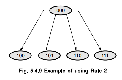
Fig.
5.4.9 shows the example for Rule 2. As shown in the Fig. 5.4.9, for state 000,
there are four next states. These states are assigned as 100, 101, 110 and 111
so that they can be grouped into logically adjacent cells in a K-map and table
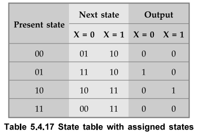
shows the state table with assigned states.
3. Choice of Flip-Flops and Derivation of Next State and Output
•
From the state assigned state table shown in Table 5.4.17, we can derive the
logic expression for the next state and output functions. But first we have to
decide on the type of flip-flops that will be used in the circuit. The most
straightforward choice is to use D flip-flops, because in this case the values
of next state are simply clocked into the flip-flops to become the new values
of present state. For other types of flip-flops, such as JK, T and RS the
relationship between the next-state variable and inputs to a flip-flop is not
as straightforward as D flip-flop. For other types of flip-flops we have to
refer excitation table of flip-flop to find flip-flop inputs. This is
illustrated in the following example.
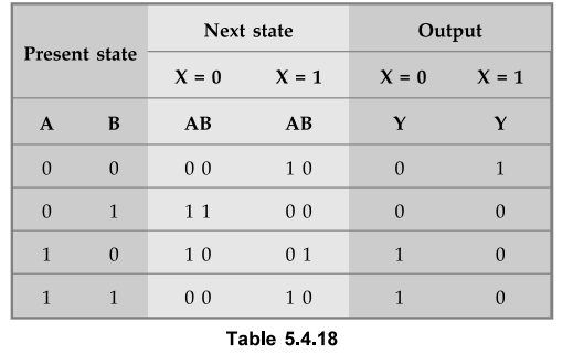
Ex.
5.4.10 A sequential circuit has one input and one output. The state diagram is
shown in Fig. 5.4.10. Design the sequential circuit with a) D flip-flops b) T
flip-flops c) RS flip-flops and d) JK- flip-flops.

Sol.
:
The state table for the state diagram shown in Fig. 5.4.10 is as given in Table
5.4.18.
As
seen from the state table there are no equivalent states. Therefore, no
reduction is the state diagram. The state table shows that circuit goes through
four states, therefore we require 2 flip-flops (number of states = 2m, where m
= number of flip-flops). Since two flip-flops are required first is denoted as
A and second is denoted as B.
1.
Design using D Flip-Flops
As
mentioned earlier, for D flip-flops next states are nothing but the new present
states. Thus, we can directly use next states to determine the flip-flop input
with the help of K-map simplification.
K-map
simplification
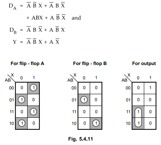
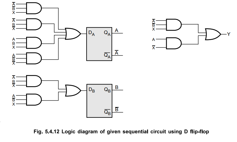
With these flip-flop input functions and circuit output function we can draw the logic diagram as follows
2.
Design using T flip-flops
Using
the excitation table for T flip-flop shown in Table 5.4.11 we can determine the
excitation table for the given circuit as shown in Table 5.4.20.
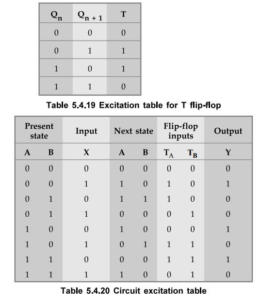
The
first row of circuit excitation table shows that there is no change in the
state for both flip-flops. The transition from 0^0 for T flip-flop requires
input T to be at logic 0. The second row shows that flip-flop A has transition
0 1. It requires the input TA to be
at logic 1. It requires the input TA to be at logic 1. Similarly, we can find
inputs for each flip-flop for each row in the table by referring present state,
next state and excitation table.
Let
us use K-map simplification to determine the flip-flop input functions and
circuit output functions.
K-map
simplification
Therefore,
input function for
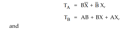
With
these flip-flop input functions and (a) For flip-flOp A circuit output function
we can draw the logic diagram as follows :
3.
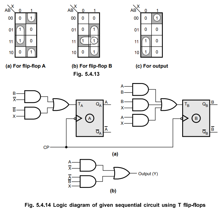
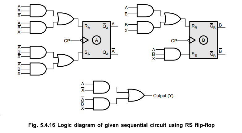
Design using RS Flip-Flops
Using
the excitation table for RS flip-flop shown in Table 5.4.21 we can determine
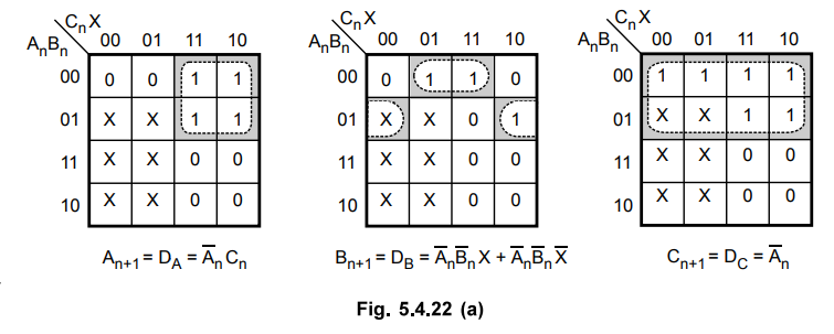
the excitation table for the given circuit as shown in Table 5.4.22.
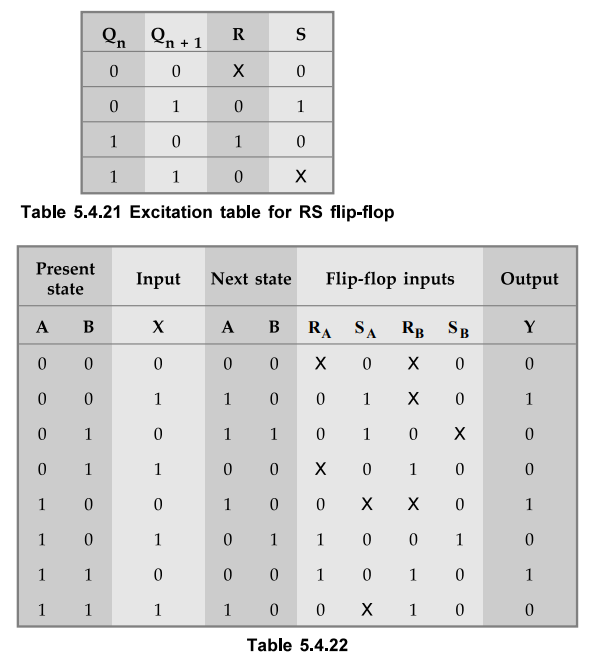
The
first row of circuit excitation table shows that there is no change in the
state for both flip-flops. The transition from 0^0 for RS flip-flop requires
inputs R and S to be X and 0, respectively. Similarly, we can determine inputs
for each flip-flop for each row in the table by referring present state, next state and excitation table. Let us
use K-map simplification to determine the flip-flop input functions and circuit
output functions.
K-map
simplification :
With
these flip-flop input functions and circuit output function we can draw the
logic diagram as follows :
4.
Design using JK Flip-Flops
Using
the excitation table for JK flop-flop shown in Table 5.4.23 we can determine
the excitation table for the given circuit as shown in Table 5.4.24.
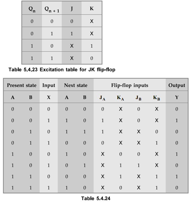
The
first row of circuit excitation table shows that there is no change in the
state for both flip-flops. The transition from 0^0 for JK flip-flop requires
inputs J and K to be 0 and X, respectively. Similarly, we can determine inputs
for each flip-flop for each row in the table by referring present state, next
state and excitation table. Let us use K-map simplification to determine the
flip-flop input functions and circuit output functions.
K-map
simplification :
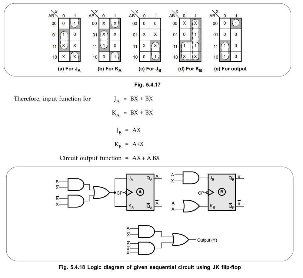
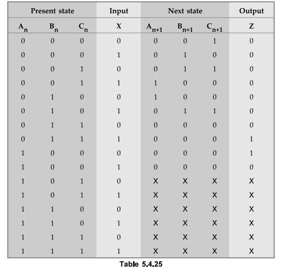
4. State Assignment Problem
Ex.
5.4.11 Design a sequential circuit for a state diagram shown in Fig. 5.4.19.
Sol.
:
Step
1 :
Assign binary values to each state. Using random state assignment we get a =
000, b = 001, c = 010, d = Oil and e =100. The excitation table with these
assignments is as given in Table 5.4.25.
Step
2 :
Find number of flip-flops needed. Since there are five states we require 2n
≥ 5 .'.n = 3 flip-flops. Let us use D flip-flops
Step
3 :
Derive the excitation table.
Step
4 :
Derive circuit output and flip-flop input functions using K-map simplification
Step
5 : State
assignment using rules.
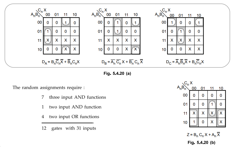
Now
we will apply the state assignment rules and compare the results. Looking at
Fig. 5.4.20 (a) and (b).
Rule
1 says that : e and d must be adjacent, and b and c must be adjacent
Rule
2 says that : b and c must be adjacent, and e and d must be adjacent
Step
6 :
Derive excitation table
Applying
Rule 1 Rule 2 to the state diagram we get the excitation table as shown in the
Table 5.4.26.
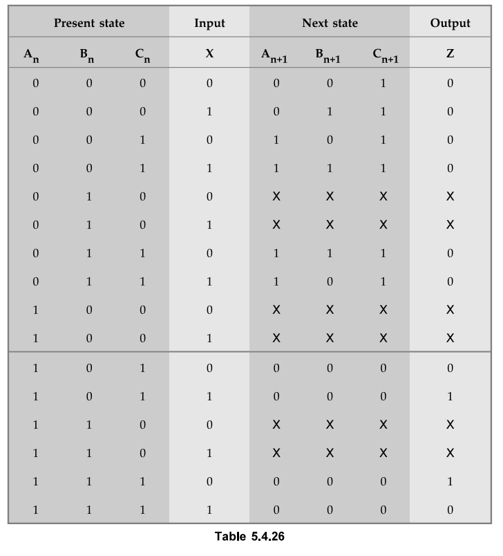
Step
7 :
Derive circuit output and flip-flop input functions using K-map simplification
The
state assignments using Rule 1 and 2 require :
Thus
by simply applying Rules 1 and 2 good results have been achieved.
5. Design with Unused States
•
There are occasions when a sequential circuit may use less than the available
these maximum number of states. We can consider the unused states as don't care
conditions and can be used to simplify the input functions to flip-flops.
•
Let us consider one example. First we will design the given sequential circuit
without using unused states and then we will design the given sequential
circuit using unused states.
Ex.
5.4.12 Design the sequential circuit for the state diagram shown in Fig. 5.4.23
use JK flip-flops.
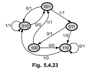
Sol.
:
Step
1 :
Derive excitation table
The
excitation table for given state diagram is as follows
Step
2 :
K-map simplification for JK inputs and circuit output
Step
3 :
Draw logic diagram.
Step
4 :
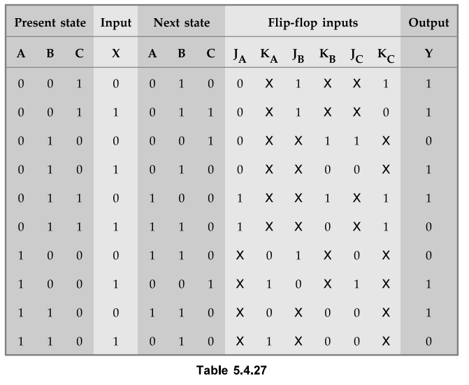
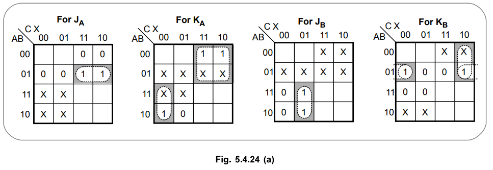
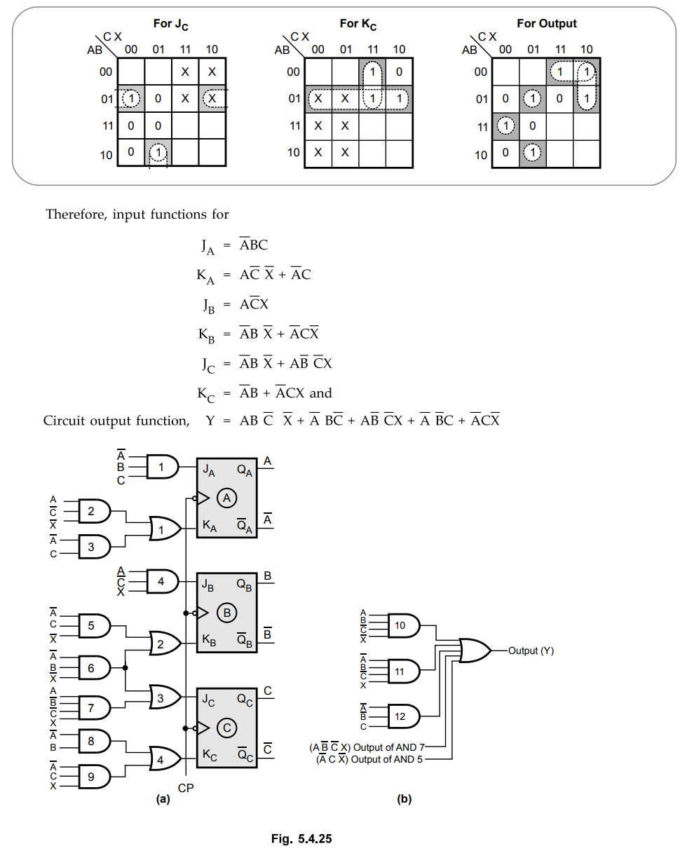
Derive circuit output and flip-flop inputs considering unused states.
Let
us see the circuit design with the use of unused states. These unused states
000, 101 and 111 are considered as a don't cares and are used to simplify the
K-maps as follows :
Step
5 :
Draw logic diagram.
•
From the above logic diagram it can be realized that using unused state as
don't cares we can further simplify the flip-flop input functions and circuit
output function.
•
One important thing neglected up to this point in the design is the initial
state of a sequential circuit. When power is turned 'ON', one cannot predict
the initial state of the flip-flops. To initialize the states of all flip-flops
to a specific states, preset and clear inputs of the flip-flops are used. These
signals are activated accordingly before the clocked operation start. This
procedure ensures the valid initial state. However, because of a noise signal
or any other unforeseen reason, if the circuit goes in an invalid state, it is
necessary to ensure that the circuit eventually goes into one of the valid
states so it can resume normal operation.
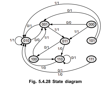
•
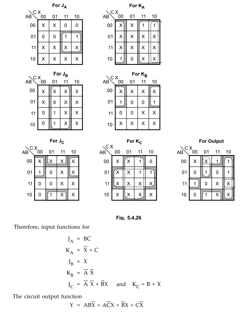
Let us analyze the previous example to see whether the next state from the
unused state is valid state or not. We know that unused states are 000, 101 and
111. These states are included in the state diagram and transitions are shown
using input functions derived from the K-maps.
•
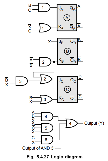
From the state diagram shown in Fig. 5.4.27 it is clear that the next state of
the unused state is a valid state for all inputs.
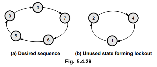
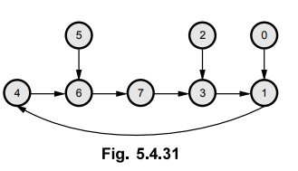
6. Lockout Condition
•
In a counter if the next state of some unused state is again an unused state
and if by chance the counter happens to find itself in the unused states and
never arrived at a used state then the counter is said to be in the lockout
conditions or deadlock conditions. This is illustrated in the Fig. 5.4.29. The
counter which never goes in lockout condition is called self starting counter.
•
The circuit that goes in lockout condition is called bushless circuit. To make
sure that the counter will come to the initial state from any unused state, the
additional logic circuit is necessary. To ensure that the lock out does not
occur, the counter should be designed by forcing the next state to be the
initial state from the unused states as shown in Fig. 5.4.30.
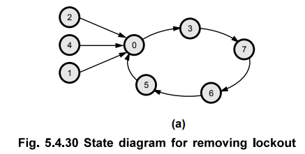
•
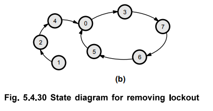
For example, as shown in Fig. 5.4.30, actually it is not necessary to force all
unused states into initial state. Forcing any one state is sufficient. Because
if counter initially goes to unused state which is not forced, it will go to
another unused state. This will continue until it reaches the forced unused
state. Once forced unused state is reached next state is used state, and
circuit is lock free circuit. This is illustrated in Fig. 5.4.30 (b).
Ex.
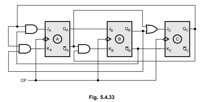
5.4.13 Design a synchronous counter for 4 → 6 → 7 → 3 → 1→ 4...
Avoid
lockout condition. Use JK type design.
Sol.
:
Step
1 :
State diagram
Here,
states 5, 2 and 0 are forced to go into 6, 3 and 1 state, respectively to avoid
lockout condition.
Step
2 :
Excitation table
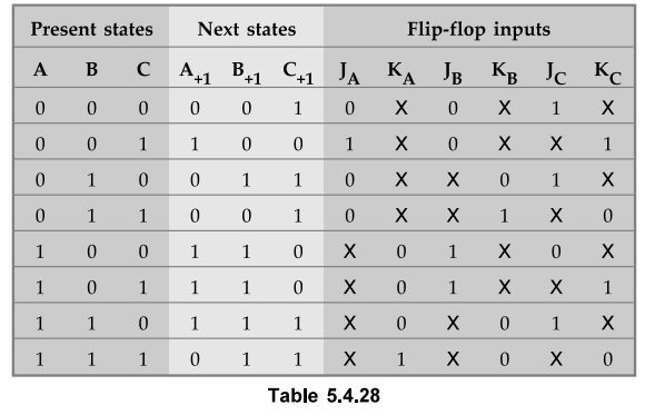
Step 3 : K-map simplification
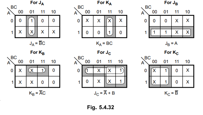
Step
4 :
Logic diagram
Examples
with Solutions
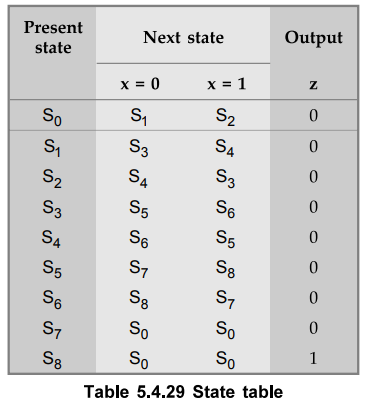
Ex.
5.4.14 For a four bit even parity bit generator, inputs come serially. The four
bits of the input sequence are to be examined by the circuit and circuit
produces a parity bit which is to be added in the original sequence. The
circuit should get ready for receiving another four bits after producing a
parity bit for the last sequence. Draw the state diagram and write down the state
transition table
Sol.
:
Step
1 :
Draw the state diagram.
The
state diagram for given problem is as shown in the Fig. 5.4.34.
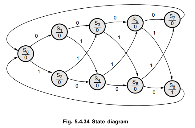
Step
2 : Determine
the Table
Step
3 :
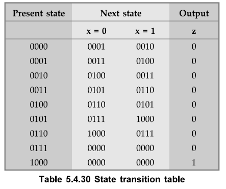
Assign states, S0 = 0000, S1 = 0001, S2 =
0010, S3 = 0011, S4 = 0100, S5 = 0101, S6
= 0110, S7 = 0111, S8 = 1000
Step
4 :
Determine the state transition table.
Ex.
5.4.15 Design a sequential circuit with 4 FF ABCD. The next states of B, C, D
are equal to the present states of A, B, C respectively. The next state of A is
equal to the EX-OR of the present states of C and D.
Sol.
:
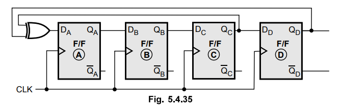
Ex.
5.4.16 Design a synchronous sequential circuit using JK for the given state
diagram.
Sol
. :
Step
1 :
Since N = 4. Number of flip-flops needed = 2
Step
2 :
Flip-flops to be used : JK
Step
3 :
Determine the excitation table.

Step
4 :
K-map simplification :
Step
5 :
Logic diagram :
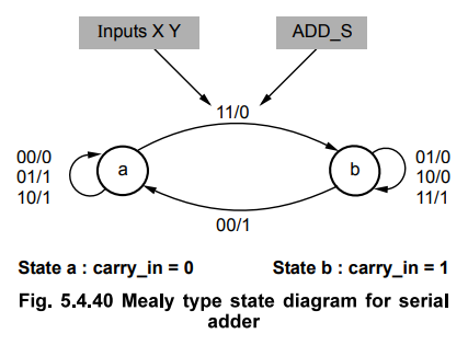
7. Serial Adder Example
•
Serial adder is a circuit in which bits are added a pair at a time. When speed
is not of great importance, it is a cost-effective option to use serial adder.
Mealy-type
FSM for Serial Adder
•
The Fig. 5.4.39 shows the block diagram of the serial adder. It includes three
shift registers that are used to hold number A, number B and sum of numbers A
and B. Shift registers A and B have parallel-load capability. Thus, we can load
values of A and B into these registers. At each clock cycle, a pair of bits is
added by the sequential circuit used as an adder, and at the end of the cycle
the resulting sum bit is shifted into the C register. Therefore, n clock cycles
are required to add n-bit number. After n clock cycles we get the output sum at
the parallel-out of shift register C.
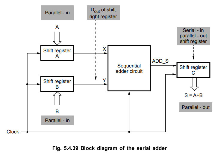
•
Here, we require a sequential adder circuit to add pair of bits from shift
registers A and B, because we have to consider the state of carry of previous
bit addition while adding the current pair of bits. The carry can have two
states either 0 or 1. Thus, we define two states as a and b to define carry
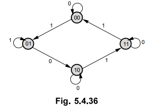
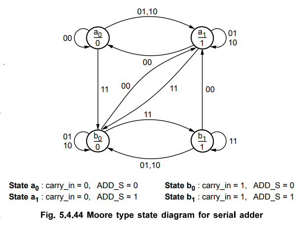
values 0 and 1, respectively. The Fig. 5.4.40 shows a state diagram, defined as
a Mealy model for adder. The output value ADD_S depends on both, the state
(carry_in) and the present values of inputs X and Y. In state a, since carry_in
is 0 we get :
ADD_S
= 0, Carry_in = 0 For XY = 00
ADD_S
= 1, Carry_in = 0 For XY = 01 or 10
ADD_S
= 0, Carry_in = 1 For XY = 11
For
XY = 11, carryjn becomes 1 and we have to change state a to b. For other values
of X and Y carry_in remains 0 and hence state does not change.
In
state b, since carryjn is 1, we get,
ADD_S
= 1, Carryjn = 0 For XY = 00,
ADD_S
= 0, Carryjn = 1 For XY = 01 or 10
ADD_S
= 1, Carryjn = 1, For XY = 11,
For
XY = 00, carry_in becomes 0 and we have to change state b to a. For other
values of X and Y carryjn remains 1 and hence state does not change. This is
illustrated in Fig. 5.4.40.
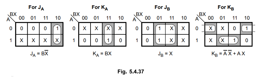
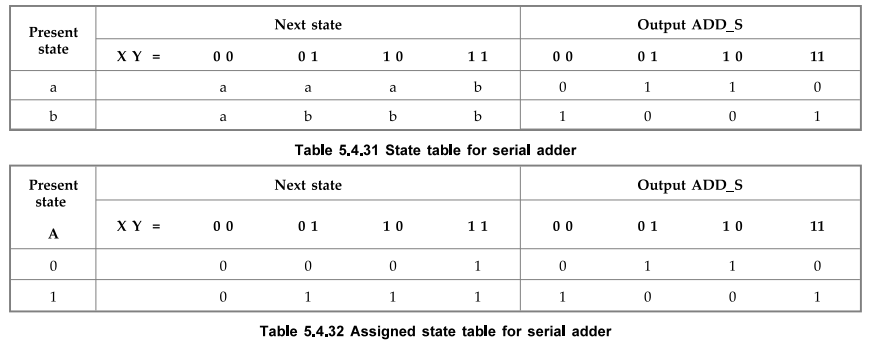
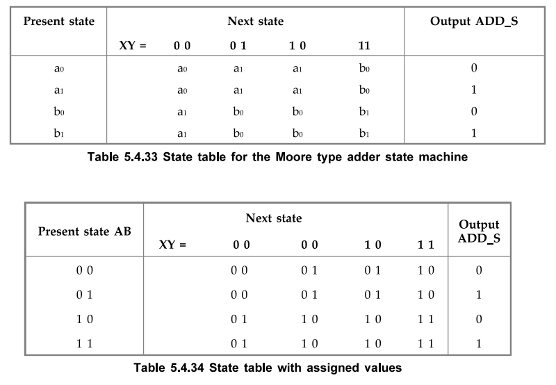
The
Table 5.4.31 shows the state table for the serial adder. A single flip-flop is
needed to represent two states. If we assign state a = 0 and state b = 1 we get
state table with assigned values as shown in Table 5.4.32.
K-map
simplification for deriving next-state and output expressions is as follows.
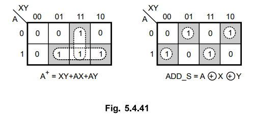
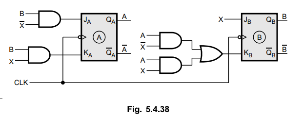
Logic
diagram
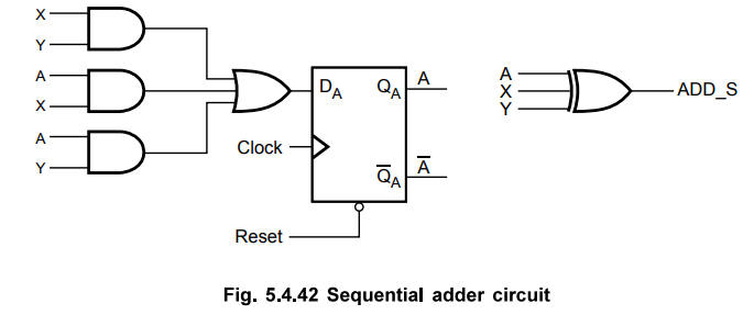
The
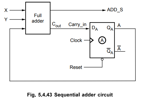
expressions for A+ and ADD_S are exactly same as the expression for
full-adder circuit. Therefore, we can represent same logic diagram as shown in
Fig. 5.4.43.
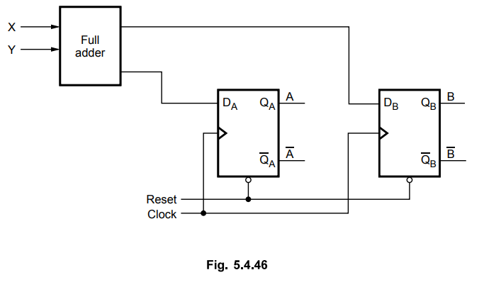
Moore
Type FSM for Serial Adder (Conversion from Mealy to Moore)
• The Fig. 5.4.4 shows state diagram for Moore type serial adder. Here, the output depends only on the state of the machine and not on inputs X and Y. Since in both states a and b, it is possible to produce two different outputs depending on the valuations of the inputs a and b, a Moore type state machine will need more than two states. We can define additional states by splitting both a and b into two states. Instead of a, we will use a0 and a2 to denote the fact that the carry is 0 and that the sum is either 0 or 1, respectively. Similarly, instead of b, we will use b0 and bx to denote the fact that the carry is 1 and that the sum is either 0 or 1, respectively. When the state is splitted, we have to direct transition associated with output 0 to state 0 and transition associated with output 1 to state 1. In our example, state a with output 1 is directed to state aj and state a with output 0 is directed to state a„. The Table 5.4.32 shows the modified Moore type state table for the serial adder. Two flip-flops are needed to represent four states. If we assign states : a0 = 00, a1 = 01, b0 = 10 and b1 = 11 we get state table with State assigned values as shown in Table 5.4.34
K-map
simplification for deriving next-state and output expressions is as follows.
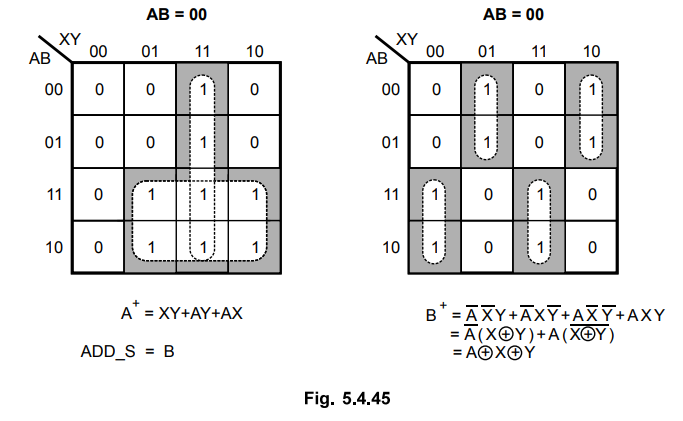
Here,
also the expressions for A and B correspond to the carry and sum expressions in
the full-adder circuit. The Fig. 5.4.46 shows the implementation of sequential
adder circuit.
Review Questions
1. Give recommended steps for the design of a clocked
synchronous sequential networks.
2. Differentiate between analysis and design of sequential logic
circuits.
3. Why is state reduction necessary ?
AU : Dec.-06, June-09, Marks 2
4. Explain the state assignment rules.
AU : May-15, Marks 2
5. What is lockout condition ?
6. What is a self starting counter
7. Design a serial adder using Mealy state model.
AU : May-16, Marks 8
8. Explain the state minimization using partitioning procedure
with a suitable example.
AU : May-16, Marks 8
9. Write the usage of merger graph with example.
Digital Logic Circuits: Unit III: (b) Analysis & Design of Synchronous Sequential Circuits : Tag: : - Design of Clock Sequential Circuits: State Assignment, Derivation of State
Related Topics
Related Subjects

Digital Logic Circuits
EE3302 3rd Semester EEE Dept | 2021 Regulation | 3rd Semester EEE Dept 2021 Regulation