Digital Logic Circuits: Unit IV: (a) Asynchronous Sequential Circuits
Design of Pulse Mode Circuit
Asynchronous Sequential Circuits
The design of pulse-mode circuits similar to the design of synchronous circuits discussed in Chapter 5.
Design of Pulse Mode Circuit
AU
: May-08, 12, June-09
The
design of pulse-mode circuits similar to the design of synchronous circuits
discussed in Chapter 5. However, when designing pulse-mode circuits, remember
that no clock pulse is present, inputs occur on only one line at a time and
only uncomplemented forms of input signals may be used.
The
absence of a clock pulse indicates that latch or flip-flop triggering must be
accomplished by utilizing the pulses on the input signals and therefore all
circuit timing information must be obtained from the input pulses. Hence, the
input pulses not only provide input information but also assume the functions
performed by the clock pulse in synchronous circuits.
The
steps involved in the design of pulse-mode asynchronous sequential circuits are
:
1.
Define states and draw a state diagram and/or state table of the circuit.
2.
Minimize the state table.
3.
Do state assignment.
4.
Choose the type of latch or flip-flop to be used and determine excitation
equations.
5.
Construct excitation table for the circuit.
6.
Determine the output equation and the flip-flop input equations using k-map
simplification.
7.
Draw the logic diagram.
Examples for Understanding
Ex.
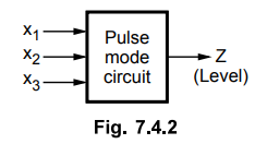
7.4.1 Design a pulse-mode circuit having two input lines, x1 and x2 and one
output line, z, as shown in Fig. 7.4.1. The circuit should produce an output
pulse to coincide with the last input pulse in the sequence x1 - x2
- x2. No other input sequence should produce an output pulse.
AU
May-08, Marks 16

Sol
. :
Step
1 :
Define states and draw the state diagram and/or state table of the circuit : S0
: indicates that the last input was x1
S1
: indicates that the sequence x1 – x2 occurred.
S2
: indicates that the sequence x1 – x2- x2
occurred.
The
Fig. 7.4.1 (a) shows the state diagram for the given circuit. It is important
to note that the format of the state diagram is similar to that used for
synchronous circuits. However, the
transitions are labeled with the input variable and the output value rather than
with both input and output values.

Also,
remember that the state transitions are triggered by the occurrence of the
indicated input pulse and not by a clock pulse.
The
state table corresponding to the state diagram of Fig. 7.4.1 (a) is as follows
:

Step
2 :
Minimize state table : State table is minimum.
Step
3 :
Assign states : A state assignment of S0 = 00, S1
= 01 and S2 = 10.
Step
4 :
Flip-flops to be used : T
Note
: For
T flip-flop output changes when T = 1.
Step
5 :
Construct execution table for the circuit.
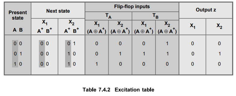
Step
6 :
K-map simplification for T inputs and Z output.
Note
:
Only vertical grouping is allowed.

Step
7 :
Draw the logic diagram.
In
the previous example, the circuit realization took the form of a Mealy-type
circuit since the output was a function of both an input and a state variable. A
next example, will now be presented that describes the realization of a
Moore-type circuit. Recall that Mealy and Moore-type circuits were defined in
Chapter 4.

Ex.
7.4.2 Design a pulse mode circuit with inputs x1, x2 , x3
and output z as shown in Fig. 7.4.2. The output should change from 0 to 1, only
for input sequence x1 – x2 – x3 occurs while Z
= 0. Also the output Z should remain in 1 until x2 occurs. Use SR
flip-flops for the design.
AU
June-09, May-12, Marks 16
Sol.
:
Step 1: Draw the state diagram and state table.

Since the output must remain high between input pulses, a Moore-type circuit is required to realize the circuit in Fig. 7.4.2. The state diagram and state table in Fig. 7.4.2 (a) and Table 7.4.3 respectively, satisfy the stated requirements.
Step
2 : Minimum state table : State table is minimum
Step
3 : Assign states : A state assignment of S0 =
00, S1 = 01, S2 = 11 and S3 = 10
Step
4 :
Flip-flops to be used : SR
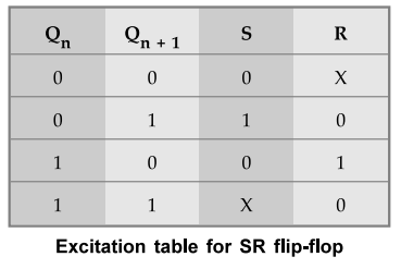
Step
5 :
Construct excitation table for the circuit.

Step
6 :
K-map simplification for SR inputs and Z output.

Step 7 : Draw the logic
diagram.

Example for Practice
Ex.
7.4.3 A pulse mode asynchronous sequential circuit has two inputs and x2, and
one output Z. An output transition from 0 to 1 occurs only when the X2 pulse
occurs in the sequence X1
– X2
– X1
– X2
The output Z resets from 1 to 0 only by the first X1
pulse that occurs following the 0 to 1 output transition. Allow overlapping
sequences. Design the circuit using T flip-flops.
Review Question
1. List the steps involved in the design of pulse-mode
asynchronous circuits.
Digital Logic Circuits: Unit IV: (a) Asynchronous Sequential Circuits : Tag: : Asynchronous Sequential Circuits - Design of Pulse Mode Circuit
Related Topics
Related Subjects

Digital Logic Circuits
EE3302 3rd Semester EEE Dept | 2021 Regulation | 3rd Semester EEE Dept 2021 Regulation