Linear Integrated Circuits: Unit I: IC Fabrication
Diffusion process of IC fabrication
The process of doping i.e. adding impurity to the silicon wafer is called diffusion. Diffusion is used to form bases, emitters and resistors in bipolar device technology and to form source and drain regions in MOS device technology.
Diffusion
The
process of doping i.e. adding impurity to the silicon wafer is called
diffusion. Diffusion is used to form bases, emitters and resistors in bipolar
device technology and to form source and drain regions in MOS device
technology. The dopant can be added into the silicon wafer by using one of the
most commonly used methods.
a)
Diffusion from a chemical source in a vapour form at very high temperature.
b)
Diffusion from doped-oxide source, and
c)
Diffusion from ion-implanted layer.
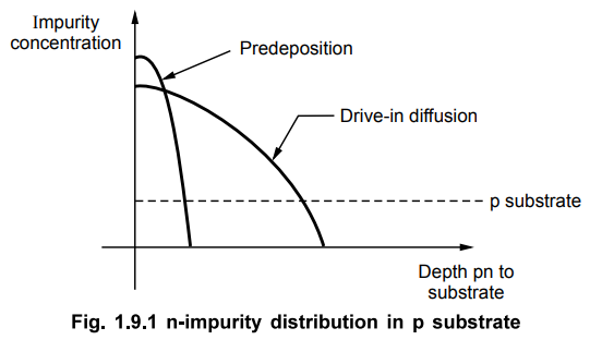
In
general, diffusion process takes place in two steps namely pre-deposition
diffusion and drive-in diffusion. In the first step, i.e. pre-deposition
diffusion step, very high concentration of dopant atoms are implanted on the
surface of silicon. These dopants or impurities are added to the surface in the
form of vapour at about 1000 °C. The bonds between the neighbouring atoms of
the silicon in the lattice are broken and the silicon atoms move out of the
lattice structure. Hence high density of vacancies is created. When dopant is
added at 1000 °C, the impurity atoms diffuse into the silicon at the locations
of vacancies. In predeposition step, a shallow, heavily doped layer of
impurities is formed at the surface. The impurity concentration is maintained
constant over the surface of the wafer. Hence it is also called constant source
diffusion. In drive-in step, the impurity atoms are redistributed. Without
adding new impurity, the present impurity atoms are driven deep into the
silicon.
As
new impurity atoms are not added during drive-in diffusion, the total amount of
impurity remains constant, the main advantage of the drive-in diffusion step is
that the surface concentration is reduced is also called constant dose
diffusion. The Fig. 1.9.1 illustrates the n impurity substrate in p substrate.
The
commonly used dopants are boron for p-type layers and phosphorus, antimony,
arsenic for n-type layers. Arsenic may also be used for n+ type source-drain
and emitter diffusions. It is observed that practically, instead of above
mentioned element, the compounds of these elements are more suitable. Such compounds
may be derived from solid, liquid or gaseous sources.
A
schematic representation of the diffusion process is as shown in the Fig.
1.9.2. The silicon wafers are stacked vertically on a movable quartz boat
inside quartz furnace tube. The temperature of the quartz furnace tube is
increased with the help of resistance heaters. The dopant to be introduced is
kept in a container. The dopant in the liquid form e.g. POCl3 may be
placed inside the quartz tube in low temperature region or preferably outside
the tube with precisely controlled temperature to maintain dopant in the liquid
form. Typically nitrogen and oxygen are used as carrier gases.

When
the carrier gases pass over the container, they carry dopant vapour into
furnace. In furnace, the gases are deposited on the silicon surface. The layer
containing silicon, oxygen, phosphorus is formed on the surface. At high
temperature such as 900 °C to 1000 °C, the dopant gets diffused into silicon.
For drive-in diffusion, the temperature is further increased to 1100 °C. So
that the dopant gets diffused with more depth in silicon. For this step, with a
proper control circuitary, the impurity supply is stopped. The proper depth can
be achieved by controlling parameters such as time and temperature of the
process.
Review Questions
1. Describe in detail about the diffusion process of IC
fabrication.
Dec.-06, 11, May-16, Marks 8
2. Explain the diffusion process as applied to IC technology.
3. What is diffusion ? Give different techniques which are
commonly used.
4. Distinguish diffusion and ion Implantation process in IC
fabrication.
Linear Integrated Circuits: Unit I: IC Fabrication : Tag: : - Diffusion process of IC fabrication
Related Topics
Related Subjects

Linear Integrated Circuits
EE3402 Lic Operational Amplifiers 4th Semester EEE Dept | 2021 Regulation | 4th Semester EEE Dept 2021 Regulation