Digital Logic Circuits: Unit I: (b) Digital Logic Families
Diode - Transistor Logic (DTL)
Circuit, Operation, Truth table, Specifications, Connection
• The Diode - Transistor Logic, DTL is somewhat more complex than RTL but because of its greater fan-out and improved noise margins it has replaced RTL.
Diode - Transistor Logic (DTL)
•
The Diode - Transistor Logic, DTL is somewhat more complex than RTL but because
of its greater fan-out and improved noise margins it has replaced RTL.
1. DTL Circuit
•
The Fig. 2.4.1 shows a discrete circuit for DTL NAND gate. It consists of input
diodes and resistor RD forming an AND gate and following them is transistor
inverter.

2. Circuit Operation
•
When both inputs are LOW, diode DA and DB conduct
resulting 0.7 volts at point P. This 0.7 voltage at point is not sufficient to
drive transistor Q1. Therefore, Q1 is cut off giving output
voltage Vo = VCC logic 1. A LOW level on any input cause
corresponding diode to conduct resulting voltage at point P = 0.7 V.
•
This causes transistor to remain in cut-off and the output voltage is equal Vcc
= logic 1. When both inputs are logic HIGH, diodes DA and DB
are reversed biased. This causes the base current of transistor Q1
to flow through RD, D1 , D2 and the base of
the transistor Q1 This drives transistor Q1 in saturation
giving output voltage = VCE(sat) = 0.2 V = logic 0.
•
For driving transistor Q1 is saturation we require more than 2.1 V
(VDl (0.7) + VD2 (0.7) + 0.7 (VBE) ) at point
P to drive transistor in saturation. Therefore, we can say that due to diodes
D1 and D2 we need increased voltage level to drive transistor in saturation.
This improves the noise margin for DTL gate.
•
When A and B inputs are HIGH, transistor Q1 is driven in saturation and its
base to emitter junction capacitance is charged. Now if any of the input goes
low, voltage at point P becomes 0.7 V and transistor Qx will try to come out of
saturation. To drive transistor from saturation to cut-off it is necessary to
discharge the stored charge on the internal capacitance. The resistance, RB
provides a discharge path for the charged stored in the transistor. Resistor RB
is connected to the - 2 V supply to increase the rate of discharge.
3. Specifications
•
Table 2.4.1 gives the specifications for DTL gate
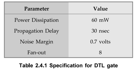
•
From the above specifications we can say that the DTL has the advantage of
greater fan-out and improved noise margins, but it suffers from somewhat lower
speed.
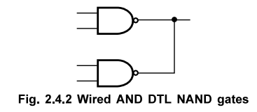
4. Wire – AND Connection
•
Like RTL, the DTL also has a capacity called wire-AND. In DTL two outputs can
be connected together as shown in the Fig. 2.4.2.
5. Modified Integrated DTL NAND Gate
AU
: May-04, 06, 07, 08, 09, 15, 16, 17,
•
To increase the fanout of DTL gate the base current of Tx has to be increased.
It is increased by replacing diode Dx by a transistor, as shown in the Fig.
2.4.3.

Review Questions
1. Draw and explain the operation of 2-input DTL NAND gate.
2. Write a note on DTL family.
3. Draw the circuit diagram of modified DTL NAND gate.
Digital Logic Circuits: Unit I: (b) Digital Logic Families : Tag: : Circuit, Operation, Truth table, Specifications, Connection - Diode - Transistor Logic (DTL)
Related Topics
Related Subjects

Digital Logic Circuits
EE3302 3rd Semester EEE Dept | 2021 Regulation | 3rd Semester EEE Dept 2021 Regulation