Digital Logic Circuits: Unit I: (b) Digital Logic Families
ECL Family
Characteristics, Basic Circuit, Advantages, Disadvantages
• Unlike TTL and CMOS families, ECL does not produce a large voltage swing between the LOW and HIGH levels. It has a small voltage swing, less than a volt, and it internally switches current between two possible paths, depending on the output state.
ECL Family
AU
: June-08, 09, 16, Dec.-06, 07, 17
•
The TTL family uses transistors operating in the saturation mode. As a result,
their switching speed is limited by the storage delay time associated with a
transistor that is driven into saturation. Another logic family has been
developed that prevents transistor saturation, thereby increasing overall
switching speed by using a radically different circuits structure, called
Current Mode Logic (CML). This logic family is also called Emitter-Coupled
Logic (ECL).
•
Unlike TTL and CMOS families, ECL does not produce a large voltage swing between
the LOW and HIGH levels. It has a small voltage swing, less than a volt, and it
internally switches current between two possible paths, depending on the output
state.
1. Characteristics of ECL Family
1.
It is the fastest of logic families. The popular 10 K and 100 K ECL families
offer propagation delays as short as 1 ns. The latest ECL family, ECL in PS
(ECL in picoseconds), offers maximum delays under 0.5 ns (500 ps).
2.
Transistors are not allowed to go into complete saturation and thus eliminating
storage delays.
3.
To prevent transistors from going into complete saturation, logic levels are
kept close to each other. Due to this transistor is not driven into saturation
when its input switches from low to high.
4.
As logic levels are kept close to each other, noise margin is reduced and it is
difficult to achieve good noise immunity.
5.
Another disadvantage of this approach is that power consumption is more because
transistors are not completely saturated.
6.
Switching transients are less because power supply current is more stable than
in TTL and CMOS circuits.
2. Basic ECL Circuit
•
The Fig. 2.7.1 shows the basic inverter/buffer circuit in ECL family. It
consists of two transistors connected in differential single ended input mode
with a common emitter resistance. The circuit has two outputs : inverting
output (OUT1) and noninverting output (OUT2). For this circuit, the input LOW
and HIGH voltage levels are defined as 3.6 V
and 4.4 V, and it produces output LOW and HIGH levels as 4.2 V and 5.0 V.
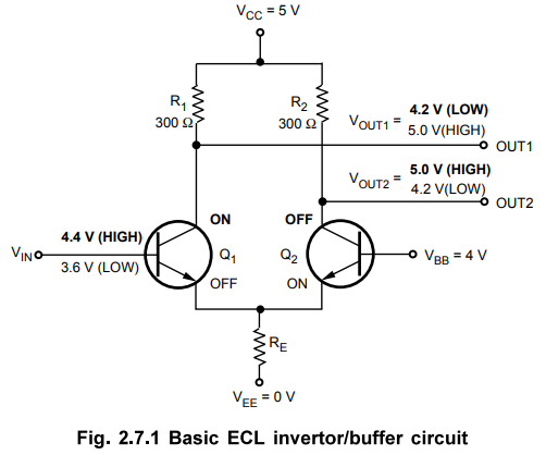
• When VIN is HIGH (4.4 V), (see
bold figures) transistor Q1 is ON, but not saturated and transistor
Q2 is OFF. Thus, VOUT2 is pulled to 5.0 V (HIGH) through
R1 and drop across R2 is 0.8 V so that VOUT2 is
4.2 V (LOW).
•
When VIN is LOW (3.6 V) (see normal figures), transistor Q2 is ON, but not
saturated and transistor Q1 is OFF. Thus, VQUT1 is pulled to 5.0 V (HIGH)
through R1 and drop across R2 is 0.8 V so that VOUT2
is 4.2 V (LOW).
3. ECL OR / NOR Gate
•
Fig. 2.7.2 shows, 2-input ECL OR/NOR gate and it logic symbol. There has an
additional transistor in parallel with Q1 as compared to ECL inverter. If any
input is HIGH corresponding transistor is active, and VQUT1 is LOW (NOR
output). At the same time Q3. is OFF producing VQUT2 HIGH (OR output).

• We can observe that the input and output LOW
and HIGH voltage levels for basic ECL family are not same, it has 0.6 V
difference. This is a problem. This problem can not be solved by connecting
diode in series with output to lower its voltage by 0.6 volt because if we does
this, it results poor fanout. Another problem occurs when output is HIGH and it
drives an another ECL input. This HIGH output has to drive base current of
another ECL input, resulting drop across R1 or R2,
reducing the output voltage. These problem of basic ECL are solved by 10 K ECL
family.

4. Advantages and Disadvantages of ECL Family
Advantages
of ECL family
1.
It is a fastest logic family. Offers propagation delay about 1 ns.
2.
Transistors are not allowed to go into complete saturation and thus eliminating
storage delays.
3.
Less switching transients since power supply current is more stable.
4.
Large fan-out.
Disadvantages
of ECL family
1.
Low noise immunity.
2.
High power dissipation.
Review Questions
1. Explain the concept and implementation of ECL
2. Write a short note on ECL family.
AU : June-08, Dec.-07, Marks 8
3. Explain the characteristics of ECL family.
4. Explain the implementation of ECL family.
AU : Dec.-06, June-09, Marks 8
5. Draw two input OR gate using ECL logic family.
6. State advantages of ECL family.
7. State disadvantages of ECL family.
8. With circuit schematic and explain the operation and
characteristics of a ECL gate.
Digital Logic Circuits: Unit I: (b) Digital Logic Families : Tag: : Characteristics, Basic Circuit, Advantages, Disadvantages - ECL Family
Related Topics
Related Subjects

Digital Logic Circuits
EE3302 3rd Semester EEE Dept | 2021 Regulation | 3rd Semester EEE Dept 2021 Regulation