Physics for Electrical Engineering: Unit II: a. Electrical Properties of Materials
Energy Bands in Solids
Electrical Properties of Materials
A set of such closely spaced energy levels is called an energy band.
ENERGY
BANDS IN SOLIDS
A
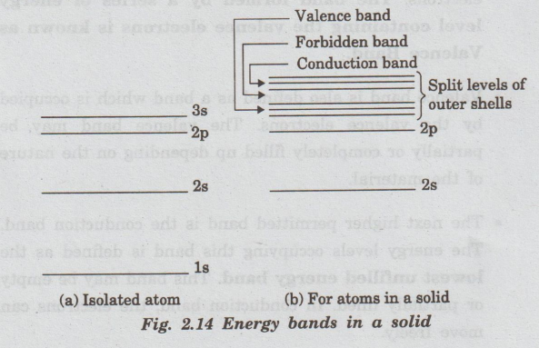
solid contains an enormous number of atoms packed closely together. In the case
of a single isolated atom, there are discrete energy levels, 1s, 2s, 2p, 3s
.... These energy levels can be occupied by the electrons of the atom, as shown
in fig. 2.14(a).
All
the atoms of a solid, if assumed isolated from one another, can have completely
identical electronic schemes of their energy levels. Then the electrons fill
the levels in each atom independently.
When
the atoms come close together, they strongly interact and the outer electron
orbitals overlap with each other.
Hence,
the interactions of large number of atoms form closely spaced energy levels
known as permitted energy band. The permitted energy bands are separated by
energy gap Eg The lower completely filled band is valence band and
upper unfilled band is called conduction band (Fig. 2.14(b)).
Definition
A set of such closely spaced energy
levels is called an energy band.
Concept of valence band, conduction
band and forbidden band
•
The energy bands in a solid correspond to the energy levels no in an atom. An
electron in a solid can have only those discrete energies that lie within these
energy bands. These bands are, therefore, called allowed energy bands.
• These (allowed) energy bands are, in
general, separated by some gaps which have no allowed energy levels. These gap (regions)
are known as forbidden energy bands.
•
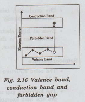
Band corresponding to valence electrons is called valence band and the band
beyond forbidden band is called conduction band, into which, the electrons
pass, and move freely.
•
The electrons in the outermost shell are called valence electrons. The band formed by a series of energy level
containing the valence electrons is known as Valence Band.
•
Valence band is also defined as a band which is occupied by the valence
electrons. The valence band may be partially or completely filled up depending
on the nature of the material.
•
The next higher permitted band is the conduction band. The energy levels
occupying this band is defined as the lowest
unfilled energy band. This band may be empty or partially filled. In conduction
band, the electrons can move freely.
•
Both conduction band and valence bands are separated by a region or gap known
as forbidden band or gap which is shown in the fig. 2.15. This band is
collectively formed by a series of energy levels above top of the valence band
and below the bottom of the conduction band.
• The energy gap between the valence band
and conduction band is called the forbidden energy gap or forbidden band
It
should be noted that no electron can exist in this band. When an electron in
the valence band absorbs enough energy, it crosses the forbidden gap and enters
into the conduction band. (Fig. 2.16)
Classification of Metals,
Semiconductors and Insulators
On
the basis of width of forbidden gap valence and conduction band the solids are
classified into insulators, semiconductors and conductors.
Insulators
•
The band structure of insulators is as shown in fig. 2.17.
•
The energy gap between conduction band and valence band is very high and is
about 10 eV.
•
The forbidden energy band is very wide. Due to this, electrons cannot jump from
valence band to conduction band. In insulator, the valence electrons are bound
very bas tightly to their parent atoms.
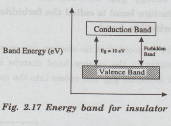
•
The conduction band is completely vacant and valence band is completely filled.
•
Even at high electric field, no electron will jump from valence band to the
conduction band because of large energy gap. Hence, the electrical conductivity
is zero.
Semiconductors
•
The band structure of semiconductors is as shown in fig. 2.18.
•
The forbidden gap is very small. Germanium and Silicon are the best examples of
semiconductors.
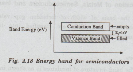
•
The energy gap between conduction band and valence band is very small. It is
about 0.5 eV to 1 eV.
•
As temperature increases, the bonds in the valence band break up and the
created electrons move from valence band to the conduction. The vacancies
created in the valence ba band due to breaking of bonds are termed as holes.
•
Hence, conduction band is partially filled and valence dale band is partially
vacant. These electrons and holes are responsible for electrical conduction.
Conductor
The
band structure of conductors is as shown in fig. 2.19.
There is no forbidden gap, both valence and
conduction bands overlap each other.
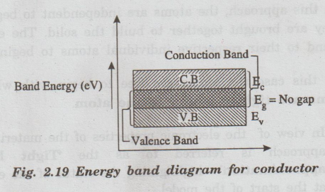
•
The electrons free to move within the conductor are responsible for electrical
conduction.
•
As temperature increases, the electrical
conduction decreases, because mobility decreases due to large number of
collisions with ions.
• The most important fact in conductors is that due to the absence of forbidden gap, there is no structure to establish holes. The total current in conductors is due to only the flow of electrons.
Physics for Electrical Engineering: Unit II: a. Electrical Properties of Materials : Tag: : Electrical Properties of Materials - Energy Bands in Solids
Related Topics
Related Subjects

Physics for Electrical Engineering
PH3202 2nd Semester 2021 Regulation | 2nd Semester EEE Dept 2021 Regulation