Electron Devices and Circuits: Review of Semiconductor Materials (Pre-requisite)
Intrinsic Semiconductors
A sample of Semiconductors in its purest form is called an Intrinsic Semiconductor. The impurity content in Intrinsic Semiconductor is very very small, of the order of one part in 100 million parts of Semiconductor.
Intrinsic Semiconductors
A
sample of Semiconductors in its purest form is called an Intrinsic
Semiconductor. The impurity content in Intrinsic Semiconductor is very very
small, of the order of one part in 100 million parts of Semiconductor.
1. Crystal Structure of Intrinsic Semiconductor
•
Consider an atomic structure of an Intrinsic Semiconductor material like
silicon. An outermost shell of an atom is caple of holding eight electrons. It
is said to be completely filled and stable, if it contains eight electrons. But
the outermost shell of an Intrinsic Semiconductor like silicon has only four
electrons. Each of these four electrons form a bond with another valence
electron of the neghbouring atoms. This is nothing but sharing of electrons.
Such bonds are called covalent bonds. The atoms align themselves to form a
three dimensional uniform pattern called a crystal.
The
crystal structure of germanium and silicon materials consists of repetitive
accurrence in three dimensions of a unit cell. This unit cell is in the form of
a tetrahedron with an atom at each vertex. But such a three dimensional structure
is used to represent a three dimensional crystal form, as shown in the Fig.
0.4.1 (a).
•
The Fig. 0.4.1 (a) shows two
dimensional representation of a germanium crystal structure. Germanium has a
total of 32 electrons. So its first orbit consists of 2 electrons, second
consists of 8, third consists of 18 and the valence shell consists of 4
electrons. As there are 4 valence electrons, it is called tetravalent atom.
•
The covalent bonds are represented by a pair of dotted lines encircling the two
electrons forming the covalent bond. The more clear understanding of the
covalent bonds can be obtained from the Fig. 0.4.1 (b) which shows the sharing
of valence electrons. Both the electrons are shared by the two atoms. Hence the
outermost shell of all the atoms is completely filled and the valence electrons
are tightly bound to the parent atoms. No free electrons are available at
absolute zero temperature.
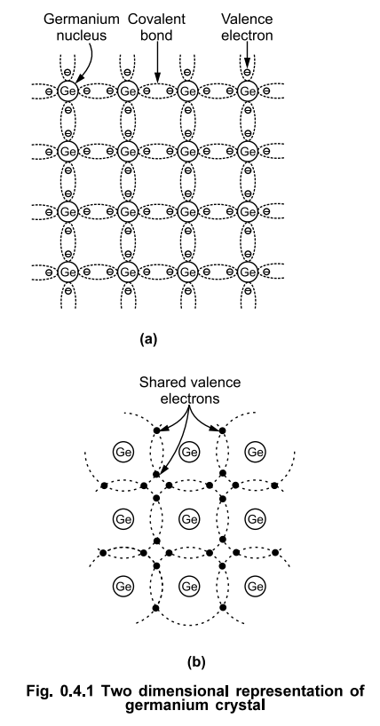
Such
an intrinsic semiconductor behaves as a perfect insulator at absolute zero
temperature.
2. Electrons and Holes in Intrinsic Semiconductors
•
Let us see what happens at room temperature. At room temperature, the number of
valence electrons absorb the thermal energy, due to which they break the
covalent bond and drift to the conduction band. Such electrons become free to
move in the crystal as shown in the Fig. 0.4.2 (a).
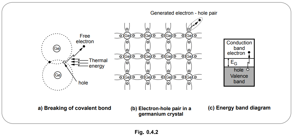
•
Once the electrons are dislodged from the covalent bonds, then they become
free. Such free electrons wander in a random fashion in a crystal. The energy
required to break a covalent bond is 0.72 eV for germanium and 1.1 eV for
silicon, at room temperature.
• When a valence electron drift from valence to conduction band breaking a covalent bond, a vacancy is created in the broken covalent bond. Such a vacancy is called a hole. Whenever an electron becomes free, the corresponding hole gets generated. So free electrons and holes get generated in pairs. The formation of electron-hole pair is shown in the Fig. 0.4.2 (b) while the corresponding energy band diagram is shown in the Fig. 0.4.2 (c). Such a generation of electron-hole pairs due to thermal energy is called thermal generation.
•
The concentration of free electrons and holes is always equal in an intrinsic
semiconductor. The hole also serves as a carrier of electricity similar to that
of free electron.
An
electron is negatively charged particle. Thus a hole getting created due to
electron drift is said to be positively charged.
3. Conduction by Electrons and Holes
•
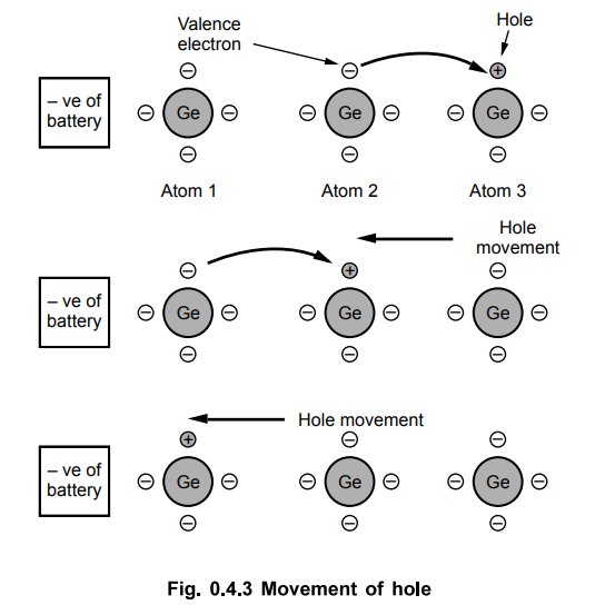
When battery is applied to an intrinsic material, free electrons move towards
positive of battery and responsible for the flow of current. This current is
called an electron current. The free electron move in conduction band.
•
Now consider three atoms of Ge in which one of the atom has a hole. Now hole is
positively charged. Then valence electron of atom 2 tries to occupy hole of
atom 3. When it does so, the hole now gets shifted to atom 2.
•
Again valence electron of atom 1 fills the hole of atom 2 and hole further
moves to atom 1.
•
Thus valence electrons move to fill the holes and holes move in opposite
direction to valence electrons. The holes keep on moving towards negative of
battery. No free electrons are involved in this action.
•
As holes are positively charged, the movement of holes cause the current called
hole current. The hole current is in opposite direction to that of an electron
current.
4. Conventional Current
•
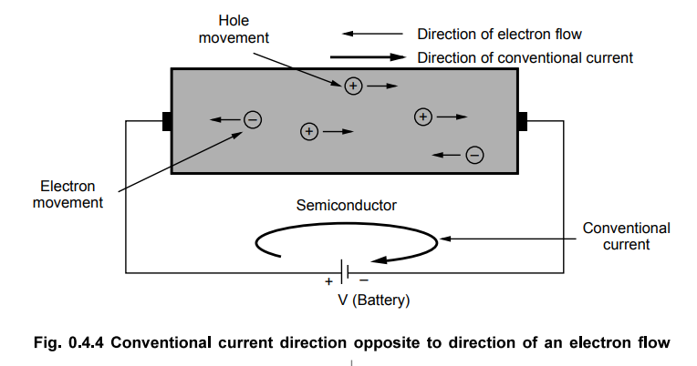
The current which flows from positive of battery to the negative of battery,
external to the battery is called a conventional current.
•
It is always the combined effect of electron and hole movement in the
semiconductors.
•
The conventional current direction is opposite to the direction of movement of
free electrons while it is same as the direction of movement of holes, in the
semiconductors.
•
Most of the electronic appliances, devices and circuits are analysed using the
flow of conventional current.
Why
intrinsic materials are not used ?
•
The conductivity of an intrinsic semiconductor at room temperature is very
small. Very few electron-hole pairs
get generated at room temperature. Similarly conductivity due to application of voltage also has
very little practical significance. Hence the intrinsic semiconductors in the
purest form is not used in practice for manufacturing of electronic devices.
Electron Devices and Circuits: Review of Semiconductor Materials (Pre-requisite) : Tag: : - Intrinsic Semiconductors
Related Topics
Related Subjects

Electron Devices and Circuits
EC3301 3rd Semester EEE Dept | 2021 Regulation | 3rd Semester EEE Dept 2021 Regulation