Electron Devices and Circuits: Review of Semiconductor Materials (Pre-requisite)
p-Type Semiconductor
Extrinsic Semiconductors
• When a small amount of trivalent impurity is added to a pure semiconductor, it is called p-type semiconductor. The trivalent impurity has three valence electrons. These elements are such as gallium, boron or indium. Such an impurity is called acceptor impurity.
p-Type Semiconductor
•
When a small amount of trivalent impurity is added to a pure semiconductor, it
is called p-type semiconductor. The trivalent impurity has three valence
electrons. These elements are such as gallium, boron or indium. Such an
impurity is called acceptor impurity.
•
Consider the formation of p-type material Pure silicon atom (4 valence
electrons ) Such p-type material formation is represented in the Fig. 0.7.1.
This means that each gallium atom added into silicon atom gives one hole. The
number of such holes can be controlled by the amount of impurity added to the
silicon. As the holes are treated as positively charged, the material is known
as p-type material.

•
At room temperature, the thermal energy is sufficient to extract an electron
from the neighbouring atom which fills the vacancy in the incomplete bond
around impurity atom. But this creates a vacancy in the adjacent bond from
where the electron had jumped, which is nothing but a hole. This indicates that
a hole created due to added impurity is ready to accept an electron and hence
is called acceptor impurity. Thus even for a small amount of impurity added,
large number of holes get created in the p-type material.
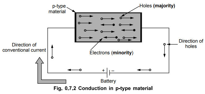
1. Conduction in p-Type Semiconductor
•
If now such p-type material is subjected to an electric field by applying a
voltage then the holes move in a valence band and are mainly responsible for
the conduction. So the current conduction in p-type material is predominantly
due to the holes. The free electrons are also present in conduction band but
are very less in number. Hence holes are the majority carriers while electrons
are minority carriers in p-type material. The conduction in p-type material is
shown in the Fig. 0.7.2.
Electron Devices and Circuits: Review of Semiconductor Materials (Pre-requisite) : Tag: : Extrinsic Semiconductors - p-Type Semiconductor
Electron Devices and Circuits: Review of Semiconductor Materials (Pre-requisite)
Under Subject

Electron Devices and Circuits
EC3301 3rd Semester EEE Dept | 2021 Regulation | 3rd Semester EEE Dept 2021 Regulation
Related Subjects
Probability and complex function
MA3303 3rd Semester EEE Dept | 2021 Regulation | 3rd Semester EEE Dept 2021 Regulation

Electromagnetic Theory
EE3301 3rd Semester EEE Dept | 2021 Regulation | 3rd Semester EEE Dept 2021 Regulation

Digital Logic Circuits
EE3302 3rd Semester EEE Dept | 2021 Regulation | 3rd Semester EEE Dept 2021 Regulation
Electron Devices and Circuits
EC3301 3rd Semester EEE Dept | 2021 Regulation | 3rd Semester EEE Dept 2021 Regulation

Electrical Machines I
EE3303 EM 1 3rd Semester EEE Dept | 2021 Regulation | 3rd Semester EEE Dept 2021 Regulation
C Programming and Data Structures
CS3353 3rd Semester EEE, ECE Dept | 2021 Regulation | 3rd Semester EEE Dept 2021 Regulation