Digital Logic Circuits: Unit II: Combinational Circuits
Introduction to Combinational Logic Circuit
Design Procedure
• When logic gates are connected together to produce a specified output for certain specified combinations of input variables, with no storage involved, the resulting circuit is called combinational logic circuit.
Introduction to Combinational Logic Circuit
AU
: Dec.-07, 08
•
When logic gates are connected together to produce a specified output for
certain specified combinations of input variables, with no storage involved,
the resulting circuit is called combinational logic circuit. In combinational
logic circuit, the output variables are at all times dependent on the
combination of input variables.

•
A combinational circuit consists of input variables, logic gates, and output
variables. The logic gates accept signals from the input variables and generate
output signals. This process transforms binary information from the given input
data to the required output data. Fig. 3.10.1 shows the block diagram of a
combinational circuit. As shown in Fig. 3.10.1, the combinational circuit
accepts n-input binary variables and generates output variables depending on
the logical combination of gates.
Review Question
1. What is combinational logic circuit ?
1. Design Procedure
AU
: Dec.-07, 08
•
The design of combinational circuits starts from the outline of the problem
statement and ends in a logic circuit diagram or a set of Boolean functions
from which the logic diagram can be easily obtained. The design procedure of
the combinational circuit involves following steps :
1.
The problem definition.
2.
The determination of number of available input variables and required output
variables.
3.
Assigning letter symbols to input and output variables.
4.
The derivation of truth table indicating the relationships between input and
output variables.
5.
Obtain simplified Boolean expression for each output.
6.
Obtain the logic diagram.
Example
for Understanding
Ex.
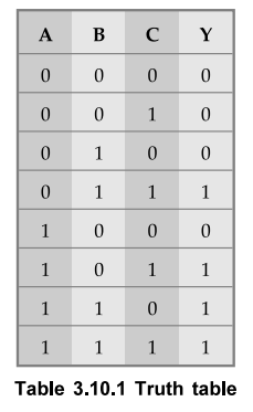
3.10.1 Design a combination logic circuit with three input variables that will
produce a logic 1 output when more than one input variables are logic 1.
Sol.
:
Step
1 :
Derive the truth table for given statement. Given problem specifies that there
are three input variables and one output variable. We assign A, B and C letter
symbols to three input variables and assign Y letter symbol to one output
variable. The relationship between input variables and output variable can be
tabulated as shown in truth Table 3.10.1.
Step
2 :
Obtain simplified Boolean expression.
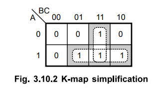
Now we obtain the simplified Boolean
expression for output variable Y using K-map simplification.
Y
= AC + BC + AB
Step
3 :
Draw logic diagram.
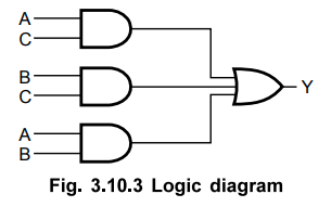
In
this chapter we are going to study various combinational circuits using above
illustrated design method.
Examples
with Solutions
Ex.
3.10.2 A majority gate is a digital circuit whose output is equal to 1 if the
majority of inputs are 1 's. The output is 0 otherwise. Using a truth table,
find the Boolean function implemented by a 3-input majority gate. Simplify the
function and implement with gates.
AU
: Dec.-07, Marks 8
Sol.
:

Ex.
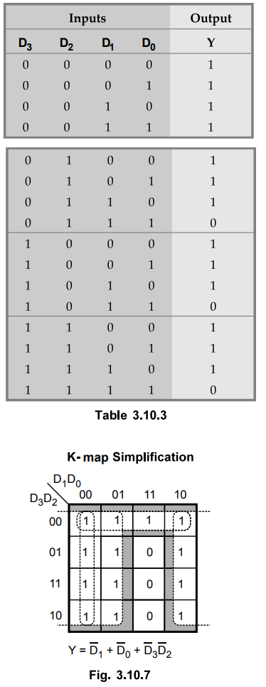
3.10.3 The inputs to a circuit are the 4 bits of the binary number D3D2D1D0.
The circuit produces a 1 if and only if all of the following conditions hold.
1)
MSB is 'T or any of the other bits are a '0'.
2)
D2 is a 1 or any of the other bits are a '0'.
3)
Any of the 4 bits are a 0.
Obtain
a minimal expression for the output.
AU
: Dec.-08, Marks 8
Sol.
:
The truth table for the given problem is as shown in Table 3.10.3.
Review Question
1. Explain the design procedure for combinational circuits.
Digital Logic Circuits: Unit II: Combinational Circuits : Tag: : Design Procedure - Introduction to Combinational Logic Circuit
Related Topics
Related Subjects

Digital Logic Circuits
EE3302 3rd Semester EEE Dept | 2021 Regulation | 3rd Semester EEE Dept 2021 Regulation