Linear Integrated Circuits: Unit I: IC Fabrication
Isolation Techniques in IC Fabrication
different techniques with diagram
We have studied that on a single silicon wafer, large number of components are fabricated. So it is important to provide isolation between these components electrically. The most commonly used isolation techniques are,
Isolation Techniques
We
have studied that on a single silicon wafer, large number of components are
fabricated. So it is important to provide isolation between these components
electrically. The most commonly used isolation techniques are,
i)
p-n junction isolation
ii)
Dielectric isolation.
The selection of the isolation technique in fabrication of any IC depends on the application of the IC i.e. for general purpose applications or specialized military applications.
1) p-n junction isolation
Consider
p-substrate with n-type epitaxial layer grown over it. To provide isolation, a
p-type impurity with high concentration (i.e. p type impurity) is diffused
selectively into an epitaxial layer such that it reaches to the p-substrate as
shown in the Fig. 1.11.1.
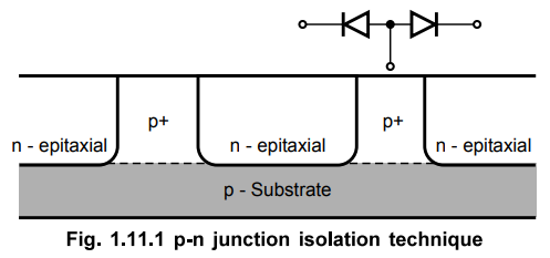
From
the Fig. 1.11.1 it is clear that n-epitaxial region forms a region which is
surrounded by p-type regions. This region is called island. Two regions are
separated by two back to back diodes as shown in the Fig. 1.11.1. These two
back to back diodes serve as isolation regions if both are reverse biased. So
when very high negative voltage is applied to p-type substrate, both the diodes
are reverse biased and thus the electrical isolation is observed between two
isolation islands.
The
important consideration for the isolation is that the concentration of the
acceptor atoms must be higher than the concentration of the p-type substrate.
If this condition is not maintained, then the depletion layer of the reverse biased
diode penentrates into the p+ region and may connect isolation islands
together.
The
main advnatage of p-n junction isolation is that different components can be
fabricated within the isolation islands. But the disadvantage of this technique
is the presence of undesirable and unavoidable parasitic capacitances at the
isolation p-n junctions. These capacitances limit high frequency performance of
the circuit. Hence this technique is generally preferred for the general
purpose ICs only.
2. Dielectric Isolation Technique
In
the dielectric isolation technique, the electrical isolation to each component
is provided by surrounding them with a solid dielectric. The most commonly used
dielectric are silicon dioxide, ruby etc. It also fulfills the purpose of physical
isolation. The dielectric layer thickness is large enough so that the parasitic
capacitances are negligible. The dielectric isolation technique is illustrated
in the Fig. 1.11.2.
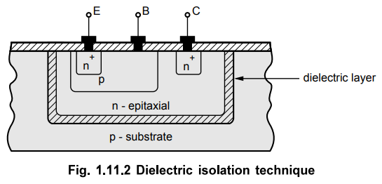
The
main advantage of the technique is that within same silicon substrate p-n-p as
well as n-p-n transistors can be fabricated.
But
the disadvantage is the increase in the cost. As the technique needs additional
steps in fabrication to deposit a dielectric layer, this technique is
expensive. Hence this technique is used for fabricating ICs for special
military applications where performance of the circuit is of prime importance
than the cost factor.
Review Questions
1. Explain the need for making isolation islands.
2. Write a note on isolation technique used in ICs.
3. Explain the importance of isolation and discuss the different
methods of isolation.
May-14, Marks 16; May-07, Marks 6
4. Compare p-n junction isolation technique with dielectric
isolation technique.
Linear Integrated Circuits: Unit I: IC Fabrication : Tag: : different techniques with diagram - Isolation Techniques in IC Fabrication
Related Topics
Related Subjects

Linear Integrated Circuits
EE3402 Lic Operational Amplifiers 4th Semester EEE Dept | 2021 Regulation | 4th Semester EEE Dept 2021 Regulation