Digital Logic Circuits: Unit I: (b) Digital Logic Families
MOS Families
Three categories, Concept, Operation, Logic circuits, Equivalent, Characteristics, Advantages and Disadvantages
Digital circuits with MOSFETs can be grouped into three categories :
MOS Families
AU
: May-04, 07, 17, June-08, Dec.-03, 06, 07, 10, 11, 14, 15, 16
Digital
circuits with MOSFETs can be grouped into three categories :
•
PMOS – uses only P-channel enhancement
MOSFETs,
•
NMOS - uses only N-channel enhancement MOSFETs,
and
•
CMOS (complementary MOS) - uses both P and N-channel devices.
•
PMOS and NMOS digital ICs are economical than CMOS ICs because they have
greater packing density than CMOS. NMOS has twice the packaging density than
PMOS. Further more, NMOS can operate at about three times faster than their
PMOS counterparts. This is because NMOS has faster moving current carriers
(electrons) whereas PMOS has slower moving current carriers (holes). CMOS has
the greatest complexity and lowest packaging density; however, it has important
advantages of high speed and much lower power dissipation. NMOS and CMOS are
widely used in the digital ICs, but PMOS ICs are no longer part of new designs.
•
CMOS circuits contain both NMOS and PMOS devices to speed the switching of
capacitive loads. It consumes low power and can be operated at high voltages,
resulting in improved noise immunity.
1. NMOS Logic
•
In this section we will see some basic NMOS logic circuits.
a.
NMOS Inverter
•
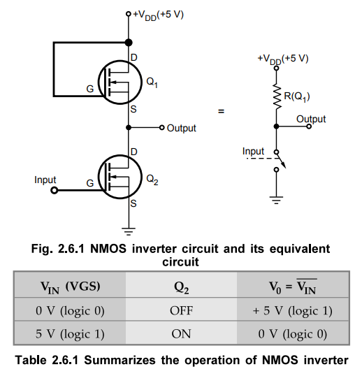
Fig. 2.6.1 shows the basic NMOS inverter circuit. It contains two N-channel MOSFETs.
Q2 is a switching MOSFET and Q1 is a load MOSFET. Qj acts
as load resistance (Rd) for Q2. As gate of Q1 is
permanently connected to the VDD, it is always ON, and hence the load
resistance is equal to the RQN of the MOSFET. Particularly, Qjis designed to
have greater RON than the RQN of Q2. To achieve this channel of Q1
is made much narrower than channel of Q2. Typically RQN of Q1
is 100 kΩ whereas RQN of Q2 is 1 kΩ. We know that MOS devices are
voltage controlled devices. When positive voltage (HIGH input) is applied
between gate and source, Q2 is switched ON and it makes the output
low. On the other hand, when input is
LOW Q2 is switched OFF and therefore, output is high.
 b.
NMOS NAND Gate
b.
NMOS NAND Gate
•
Fig. 2.6.2 shows 2-input NMOS NAND gate. Q1 acts as a load resistors
and Q2 and Q3 are the switching MOSFETs controlled by the
inputs A and B. Fig. 2.6.2 (b) shows the equivalent switching circuit, consisting
of a resistor and two switches in series.
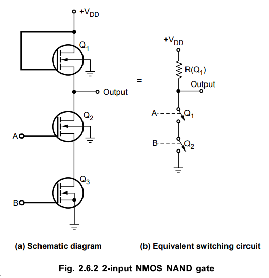
If
either A or B or both inputs are low, the corresponding MOSFETs are OFF i.e,
the corresponding switches are open and the output is high. If A and B both
inputs are high, the corresponding MOSFETs are ON i.e, the corresponding
switches are closed and the output is low.
c.
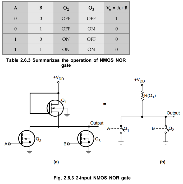
NMOS NOR Gate
•
Fig. 2.6.3 shows 2-input NMOS NOR gate. Qj acts as a load resistor and Q2 and
Q3 are the switching MOSFETs controlled by the inputs A and B. Fig. 2.6.3 (b) shows the equivalent switching circuit,
consisting of a resistor and two switches connected in parallel. When either or
both input are high, the corresponding MOSFETs are ON i.e, corresponding
switches are closed making the output low. If both inputs are low, both MOSFETs
are OFF i.e, both switches are open and the output is high.
d.
Characteristics of NMOS
Operating
speed :
•
Low operating speed with propagation delay time around 50 ns. This is because
it has high output resistance, very high input resistance and reasonably high
input capacitance.
Noise
margin : Typically 1.5 V
Fan
out : Typically 30
Power
drain : Less, around 0.1 mW per gate.
2. PMOS Logic
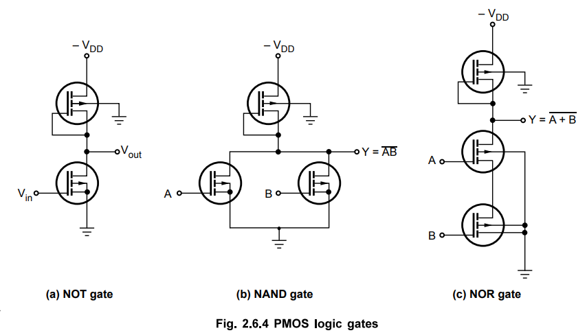
•
The Fig. 2.6.4 shows PMOS inverter, NAND gate and NOR gate. For P-channel,
enhancement-type MOSFET a negative voltage is needed at the gate terminal to
form a channel. According to the positive logic, logic-0 is approximately – VDD
< - VT, which is the low-voltage signal value, while logic-1 is
approximately ground, which is the high voltage signal value.
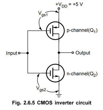
3. CMOS Inverter
•
Fig. 2.6.5 shows the basic CMOS inverter circuit. It consists of two MOSFETs in
series in such a way that the p-channel device has its source connected to +
VDD (a positive voltage) and the n-channel device has its source connected to
ground. The gates of the two devices are connected together as the common input
and the drains are connected together as the common output.
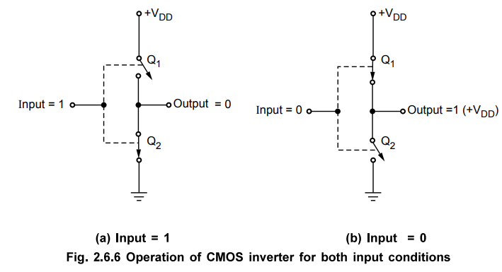
1. When input is HIGH, the gate of Q2
(p-channel) is at 0 V relative to the source of Q1 i.e. VgSl = 0 V. Thus, Qx is
OFF. On the other hand, the gate of Q2 (n-channel) is at +VDD relative to its
source i.e. VgS2 = +VDD. Thus, Q2 is ON. This will produce VOUT ~ 0
V, as shown in the Fig. 2.6.6 (a).
2.
When input is LOW, the gate of Qx (p-channel) is at a negative potential
relative to its source while Q2 has Vgs = 0 V. Thus, is ON and Q2 is OFF. This
produces output voltage approximately + VDD, as shown in the Fig. 2.6.6 (b).
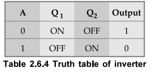
•
Table 2.6.4 summarizes the operation of CMOS inverter circuit.
•
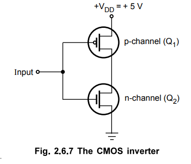
The Fig. 2.6.7 shows, different symbols used for the p-channel and n-channel transistors
to reflect their logical behaviour. The n-channel transistor (Q2) is switched
'ON' when a HIGH voltage is applied at the input. The p-channel transistor (Qi)
has the opposite behaviour, it is switched ON when a LOW voltage is applied at
the input. It is indicated by placing bubble in the symbol.
•
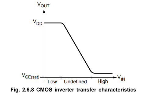
The Fig. 2.6.8 shows the transfer characteristics of CMOS inverter.
4. COMS NAND Gate
•
Fig. 2.6.9 shows CMOS 2-input NAND gate. It consists of two p-channel MOSFETs,
Q4 and Q2, connected in parallel and two n-channel MOSFETs, Q3 and Q4 connected
in series.
•
Fig. 2.6.9 (a) shows the equivalent switching circuit when both inputs are low.
Here, the gates of both p-channel MOSFETs are negative with respect to their
sources, since the sources are connected to + VDD. Thus, Qj and Q2 are both ON.
Since the gate-to-source voltages of Q3 and Q4 (n-channel MOSFETs) are both 0
V, those MOSFETs are OFF. The output is therefore connected to +VDD (HIGH) through
Q4 and Q2 and is disconnected from ground, as shown in the Fig. 2.6.9 (b). Fig.
2.6.9 (c) shows the equivalent switching circuit when A = 0 and B = +VDD. In
this case, Q4 is on because VGSi= - VDD and Q4 is ON because VGg4 = +VDD.
MOSFETs Q2 and Q3 are off because their gate-to-source voltages are 0 V. Since
Q4 is ON and Q3 is OFF, the output is connected to +VDD and it is disconnected
from ground. When A = +VDD and B = 0 V, the situation is similar (not shown);
the output is connected to +VDD through Q2 and it is disconnected from ground
because Q4 is OFF. Finally, when both inputs are high (A = B = +VDD), MOSFETs
Qj and Q2 are both OFF and Q3 and Q4 are both ON. Thus, the output is connected
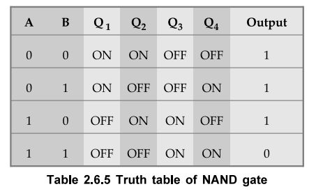
to the ground through Q3 and Q4 and it is disconnected from + VDD. The Table
2.6.5 summarizes the operation of 2-input CMOS NAND gate.
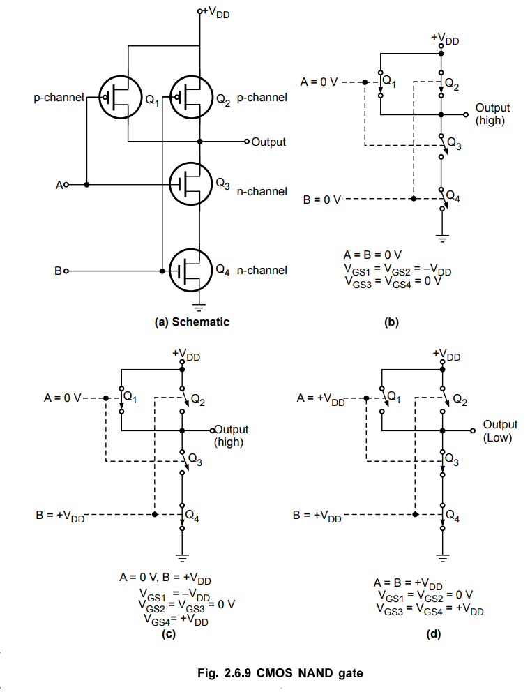
Note
:
p-channel MOSFET is ON when its gate voltage is negative with respect to its
source whereas n-channel MOSFET is ON when its gate voltage is positive with
respect to its source
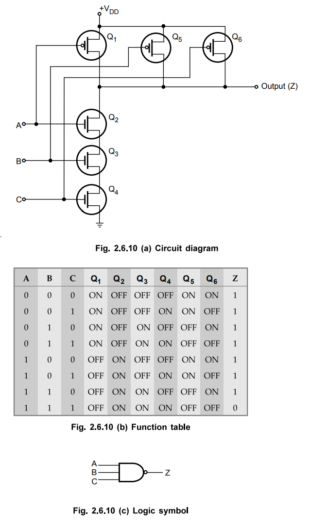
•
The Fig. 2.6.10 shows the circuit diagram, function table and logic symbol of
CMOS 3-input NAND gate.
5. CMOS NOR Gate
•
Fig. 2.6.11 shows 2-input CMOS NOR gate. Here, p-channel MOSFETs and Q2 are
connected in series and n-channel MOSFETs Q3 and Q4 are connected in parallel.
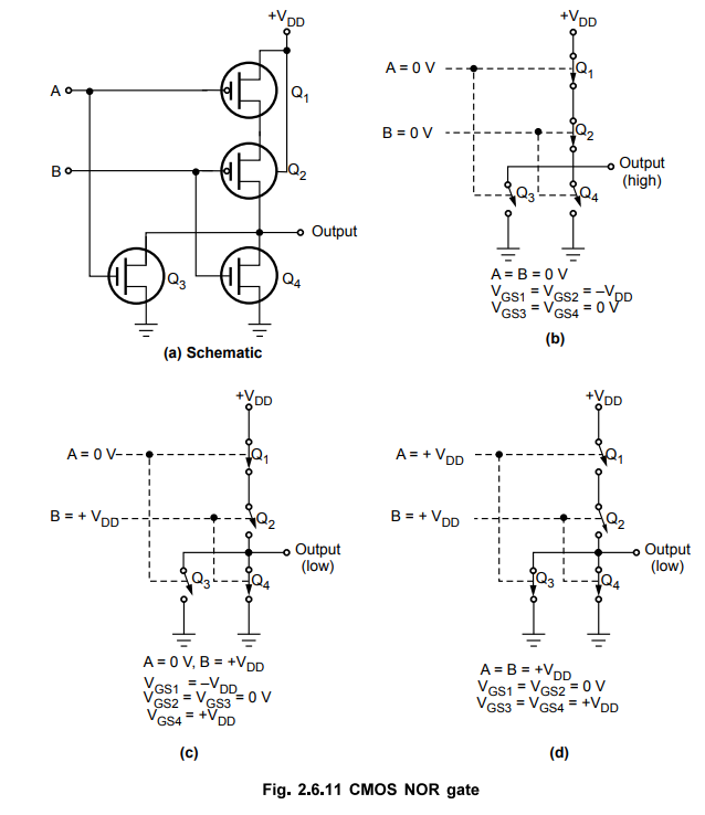
•
Like NAND circuit, this circuit can be analyzed by realizing that a LOW at any
input turns ON its corresponding p-channel MOSFET and turns OFF its
corresponding n-channel MOSFET, and vice versa for a HIGH input. This is
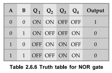
illustrated in Fig. 2.6.11. The Table 2.6.6 summarizes the operation of 2-input
NOR gate.
6. Characteristics of CMOS Family
•
Operating Speed : Slower than TTL series. Approximately
25 to 100 ns depending on the subfamily of CMOS. It also depends on the power
supply voltage.
•
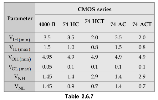
Voltage Levels and Noise Margins : The voltage levels for
CMOS varies according to their subfamilies. These are listed in Table 2.6.7.
Noise margins in table are calculated as follows.
VNH
= VOH(min) - VIH(min)
VNL
= VIL(max) - VOL(max)
•
Fan-out : The CMOS inputs have an extremely large resistance
(1012 Ω) that draws essentially no current from the signal source.
Each CMOS input, however, typically presents a 5 pF load to ground as shown in
the Fig. 2.6.12. This input capacitance limits the number of CMOS inputs that
one CMOS output can drive.
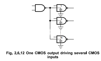
•
The CMOS output has to charge and discharge the parallel combination of all the
input capacitances. This charging and discharging time increases as we increase
number of loads. Typically, each CMOS load increases the driving circuit's
propagation delay by 3 ns. Thus, fan-out for CMOS depends on the permissible
maximum propagation delay. Typically, CMOS outputs are limited to a fan-out of
50 for low-frequency operation (≤ 1 MHz). Of course, for high-frequency
operation the fan-out would have to be less.
•
Power Dissipation (PD) : The power dissipation
of a CMOS IC is very low as long as it is in a d.c. condition. Unfortunately,
power dissipation of CMOS IC increases in proportion to the frequency at which
the circuits are switching states. For example, a CMOS NAND gate that has PD
= 10 nW under d.c. conditions will have PD = 0.1 mW at a frequency of 100 kHz
and 1 mW at 1 MHz.
•
When CMOS output switches from LOW to HIGH, a transient charging current has to
be supplied to the load capacitance. Therefore, as the switching frequency
increases, the average current drawn from VDD also increases,
resulting increase in power dissipation.
•
Propagation Delay : The propagation delay in CMOS is the
sum of delay due to internal capacitance and due to load capacitance. The delay
due to internal capacitance is called the intrinsic propagation delay. The
delay due to load capacitance can be approximated as follows.
tp(CL)
≈ 0.5 RQ CL seconds
where
tp(CL) is either tpLH or tpHL
Ro
is the output resistance of the gate and CL is the total load
capacitance.
The
Ro depends on the supply voltage and it can be approximated as
Ro
≈
VCC / Ios
where
Ios is the short circuit output current.
•
Unused Inputs : CMOS inputs should never be left disconnected.
All CMOS inputs have to be tied either to a fixed voltage level (0 V or VDD) or
to another input. This rule applies even to the inputs of extra unused logic
gates on a chip. An unused CMOS input is susceptible to noise and static charges
that could easily bias both the P and N-channel MOSFETs in the conductive
state, resulting in increased power dissipation and possible overheating.
Static-charge
Susceptibility (CMOS Hazards) : Every CMOS device is
vulnerable to the building up of electrical charge on its insulated gate.
Recall that the relationship between charge Q and voltage V on a capacitor
having capacitance C is
V
= Q / C
•
Since the input capacitance at the gate is usually quite small (a few
picofarads), a relatively small amount of charge can create a large voltage
which may be greater than the breakdown voltage of a MOS gate (typically 100
V).
•
The primary source of charge is "static" electricity, usually
produced by handling and the motion of various kinds of plastics and textiles.
The CMOS devices are protected against this static charge by on-chip
diode-resistor network, as shown in the Fig. 2.6.13. These diodes are designed
to turn ON and limit the size of the input voltage to well below any damaging
value.

•
Latch-up : CMOS integrated circuits contain parasitic PNP and
NPN transistors : transistors that exist because of the proximity of P and N
materials embedded in the substrate. Their existence is not intentional but is
unavoidable. Because of conducting paths between a pair of such transistors, a
device can be triggered into a heavy conduction mode, known as latch-up. This
heavy conduction mode, results large current flow which can destroy IC. Most
CMOS circuits contain protective measures to prevent latch-up, but it can still
occur if the manufacturers specified maximum ratings are exceeded.
7. Advantages and Disadvantages of CMOS Family
Advantages
1.
Consumes less power.
2.
Can be operated at high voltages, resulting in improved noise immunity.
3.
Fan-out is more.
4.
Better noise margin.
Disadvantages
1.
Susceptible to static charge.
2.
Switching speed low.
3.
Greater propagation delay.
Review Questions
1. Write a note on NMOS logic.
2. Write a note on PMOS logic.
3. Explain the concept, operation and characteristics of CMOS
technology.
4. Write a short note on CMOS family.
AU : Dec.-07, Marks 8
5. Explain the CMOS inverter.
6. Sketch the typical transfer characteristics of a CMOS
inverter.
7. Draw the circuit of a CMOS two input NAND gate and explain
its operation.
AU : Dec.-03, June-08, Marks 8
8. Draw and explain CMOS NAND gate.
9. Draw and explain the circuit diagram of a CMOS NOR gate.
10. Explain the characteristics of CMOS family.
AU : Dec.-06, 11, May-07, Marks 8
11. State the advantages and disadvantages of CMOS family.
12. Draw the MOS logic circuit for NOT gate and explain its operation.
13. Explain with an aid of circuit diagram the operation of 2
input CMOS NAND gate and list out its advantages over other logic families.
AU : Dec.-16, Marks 10
Digital Logic Circuits: Unit I: (b) Digital Logic Families : Tag: : Three categories, Concept, Operation, Logic circuits, Equivalent, Characteristics, Advantages and Disadvantages - MOS Families
Related Topics
Related Subjects

Digital Logic Circuits
EE3302 3rd Semester EEE Dept | 2021 Regulation | 3rd Semester EEE Dept 2021 Regulation