Physics for Electrical Engineering: Unit IV: Optical Properties of Materials
Optical Processes in Quantum wells
The basic properties of a quantum well is understood from the simple 'particle in a box' model. In quantum well an isolated thin semiconductor sheet of thickness L is considered as length of the box.
OPTICAL PROCESSES IN QUANTUM WELLS
The
term "Well" refers to a semiconductor region that is grown to
possess a lower energy, so that it acts as a trap for electrons and holes.
These are called quantum wells because these semiconductor regions are only a
few atomic layers thick. Quantum wells are real-world implementation of
the "particle in one-dimensional box" problem.
The
basic properties of a quantum well is understood from the simple 'particle in a
box' model. In quantum well an isolated thin semiconductor sheet of thickness L
is considered as length of the box.
Solving
the Schroedinger equation and applying boundary conditions result in the
following quantized energies for charge
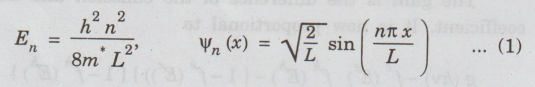
n
= 1, 2, ... ∞ Quantum numbers
h
- Planck's constant
m
- mass of charge carrier (electron or hole)
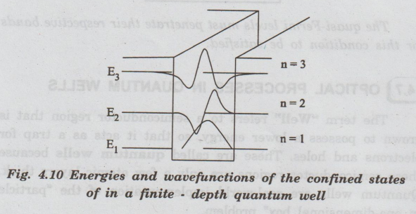
Finite
quantum wells are formed by sandwiching a thin layer (<50 nm) of one
semiconductor (GaAs) between two layers of another larger band gap
semiconductor (AlGaAs) barriers. This finite depth potential well is shown in
fig. 4.10.
The
fig. 4.10 shows energies and wave functions for a finite depth well. The energy
of the first allowed electron energy level in a typical 100 Å GaAs quantum well
is about 40 meV calculated using eqn (1).
The
optical transition is proportional to the density of states at the initial
point in the valence band and the final point in the conduction band.
The
energy absorption spectrum therefore exhibits a very different form for
nanostructures of different dimensionality.
In
quantum wells for confined the direction instead of momentum conservation a
selection rule applied. This rule states that only transition between states of
the same quantum number in the VB and CBs are allowed.
This
rule follows from the fact that the optical absorption strength is proportional
to the overlap integral of the conduction and valence wavefunctions. (Fig.
4.11)
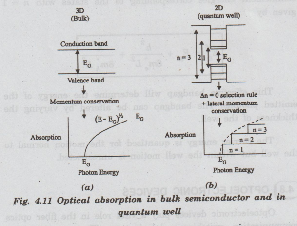
In
quantum well the electrons and holes are still free to move in the directions
parallel to the layers. Therefore, there is deviation in discrete energy states
for electrons and holes.
There
are 'subbands' that start at corresponding to each of the energies calculated
for the confined states.
The
density of state turns out to be a 'step' that starts at the appropriate
confinement energy.
Optical
transitions must still conserve momentum in this direction and just as for bulk
semiconductors. The optical absorptions must still therefore follow the density
of states. Hence in this simple model, the optical absorption in a quantum well
is a series of steps with one step for each quantum number 'n' as shown in fig.
4.11 (b).
As
a consequence of quantum confinement in quantum well, the effective band gap of
a semiconductor Eefg increases from its bulk value by the
addition of the electron and hole confinement energies corresponding to the
states with n = 1 given by
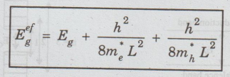
This
effective bandgap will determine the energy of the emitted photons. The bandgap
can be altered by varying the thickness of the well.
The
carrier energy is quantised for the motion normal to the well but within the
well motion is unrestricted.
Physics for Electrical Engineering: Unit IV: Optical Properties of Materials : Tag: : - Optical Processes in Quantum wells
Physics for Electrical Engineering: Unit IV: Optical Properties of Materials
Under Subject
Physics for Electrical Engineering
PH3202 2nd Semester 2021 Regulation | 2nd Semester EEE Dept 2021 Regulation
Related Subjects

Professional English II
HS3251 2nd Semester 2021 Regulation | 2nd Semester Common to all Dept 2021 Regulation
Statistics and Numerical Methods
MA3251 2nd Semester 2021 Regulation M2 Engineering Mathematics 2 | 2nd Semester Common to all Dept 2021 Regulation

Engineering Graphics
GE3251 eg 2nd semester | 2021 Regulation | 2nd Semester Common to all Dept 2021 Regulation
Physics for Electrical Engineering
PH3202 2nd Semester 2021 Regulation | 2nd Semester EEE Dept 2021 Regulation

Basic Civil and Mechanical Engineering
BE3255 2nd Semester 2021 Regulation | 2nd Semester EEE Dept 2021 Regulation
Electric Circuit Analysis
EE3251 2nd Semester 2021 Regulation | 2nd Semester EEE Dept 2021 Regulation

Physics for Electronics Engineering
PH3254 - Physics II - 2nd Semester - ECE Department - 2021 Regulation | 2nd Semester ECE Dept 2021 Regulation

Electrical and Instrumentation Engineering
BE3254 - 2nd Semester - ECE Dept - 2021 Regulation | 2nd Semester ECE Dept 2021 Regulation
Circuit Analysis
EC3251 - 2nd Semester - ECE Dept - 2021 Regulation | 2nd Semester ECE Dept 2021 Regulation

Materials Science
PH3251 2nd semester Mechanical Dept | 2021 Regulation | 2nd Semester Mechanical Dept 2021 Regulation

Basic Electrical and Electronics Engineering
BE3251 2nd semester Mechanical Dept | 2021 Regulation | 2nd Semester Mechanical Dept 2021 Regulation

Physics for Civil Engineering
PH3201 2021 Regulation | 2nd Semester Civil Dept 2021 Regulation

Basic Electrical, Electronics and Instrumentation Engineering
BE3252 2021 Regulation | 2nd Semester Civil Dept 2021 Regulation

Physics for Information Science
PH3256 2nd Semester CSE Dept | 2021 Regulation | 2nd Semester CSE Dept 2021 Regulation

Basic Electrical and Electronics Engineering
BE3251 2nd Semester CSE Dept 2021 | Regulation | 2nd Semester CSE Dept 2021 Regulation

Programming in C
CS3251 2nd Semester CSE Dept 2021 | Regulation | 2nd Semester CSE Dept 2021 Regulation