Digital Logic Circuits: Unit V: VHDL
Organization of Structuural Description
VHDL
• The listing shows the VHDL structural description for half-adder. In the VHDL description, the entity part is same as that of behavioral description. However, architecture part has two components : declaration and instantiation.
Organization of Structuural Description
•
The listing shows the VHDL structural description for half-adder. In the VHDL
description, the entity part is same as that of behavioral description.
However, architecture part has two components : declaration and instantiation.
1. Component Declaration
•
In declaration part all different components used in the system description are
declared. The syntax for component declaration is
component
component-name
Port
(port list);
end
component;
For
example, following description declares AND gate component.
component
and2
port
( II, 12 : in std_logic;
O1
: out std_logic);
end
component;
The
and2 components has two inputs : Il and 12 and one output Ol. Once the
component is declared we can use the same component one or more times in the
system description.
2. Component Instantiation
•
The instantiation part of the code maps the geneic inputs/outputs to the actual
inputs/outputs of the system. The format of a component statement is :
component_label
: component name port map(association list);
•
For example, the statement and2 port map (A, B, Cout); maps A to input II of
and2, input B to input 12 of and2, and output Cout to output O1 of and2. This
mapping means that the logic relationship between A, B and Cout is the same as
between II, I2 and O1.
Listing
10.9.1 : VHDL structural description.
library
ieee;
use
ieee.std_logic_1164.all;
entity
half_adder is
port
( A, B : in std_logic;
Sum,
Cout: out std_logic);
end
half_add;
architecture
adder of half_adder is
..
Component Declaration
component
xor2
port
( II, 12 : in std_logic;
O1:
out std_logic);
end
component;
component
and2
port
( II, 12 : in std_logic;
Ol
: out std_logic);
end
component;
begin
..
Statements instantiation
XI
: xor2 port map (A, B, Sum);
A1
: and2 portmap (A, B, Cout);
end
adder;
•
The VHDL part of listing 10.9.1, does not give the complete code for
half_adder. It does not specify the function of the components and2 and xor2.
To specify and2 as an AND gate or xor2 as an XOR gate, we have to link the
entity having the same name as component which specifies the relationship
between II, 12 and Ol as AND gate or XOR gate, respectively. This is
illustrated in Listing 10.9.2.
Listing
10.9.2 : VHDL code of half adder,
library
ieee;
use
ieee.std_logic_1164.all;
entity
xor2 is
port(Il,
12 : in std_logic;
Ol
: out std_logic);
end
xor2;
architecture
xor_gate of xor2 is
begin
O1
<= I1 xor I2;
end
xor_gate;
library
ieee;
use
ieee.std_logic_1164.all;
entity
and2 is
port
(II, 12 : in std_logic; Ol : out std_logic);
end
and2;
architecture
and gate of and2 is
begin
O1
< = I1 and I2;
end
and_gate;
library
ieee;
use
ieee.std_logic_1164.all;
entity
half_adder is
port
( A, B : in std_logic;
Sum,
Cout: out std_logic);
end
half_adder;
architecture
adder of half_adder is
component
xor2
port
( II, 12 : in std_logic;
O1
: out std_logic);
end
component;
component
and2
port
( I1, I2 : in std_logic;
O1
: out std_logic);
end
component;
begin
XI
: xor2 port map (a, b, S);
A1
: and2 port map (a, b, C);
end
adder;
3. VHDL Program Examples
Listing 10.9.3 : VHDL code for the half adder,
library ieee;
use
ieee.std_logic_1164.all;
entity
I2_O2 is
port
( II, 12 : in std_logic;
Ol,
02 : out std_logic);
end
I2_O2;
architecture
HA of I2_O2 is
component
xor2
port
( II, 12 : in std_logic;
Ol
: out std_logic);
end
component;
component
and2
port
( II, 12 : in std_logic;
Ol
: out std_logic);
end
component;
for
A1 : and2 use entity work.two_input (and2_4);
for
XI : xor2 use entity work.two_input (xor2_4);
begin
XI
: xor2 port map (II, I2, O1);
A1
: and2 port map (I1, I2, O2);
end
HA;
Listing
10.9.4 : VHDL description of a full adder.
library
ieee;
use
ieee.std_logic_1164.all;
entity
full_adder is
port
( A, B, Cin : in std_logic;
Sum,
Cout: out std_logic);
end
full_adder;
architecture
adder of full_adder is
component
HA
port
( II, 12 : in std_logic;
Ol,
02 : out std_logic);
end
component;
component
or2
port
( II, 12 : in std_logic;
Ol
: out std_logic);
end
component;
for
all : HA use entity work.I2_O2 (HA);
for
all : or2 use entity work.two_inout (or2_4);
signal
SO, CO, Cl : stdlogic;
begin
HA1
: HA port map (A, B, S0, C0);
HA2
: HA port map (Cin, S0, Sum, C1);
OR1
: or2 port map (C0, C1, Cout);
end
adder;
Listing
10.9.5 : HDL description of a 2 x 1 multiplexer with active low enable,
library
ieee;
use
ieeeR.std_logic_1164.all;
entity
mux2 × 1 is
port
( DO, DI, S, Enbar : in std_logic;
Y
: out std_logic);
end
mux2 × 1;
architecture
MUX of mux2 × 1 is
-
Components declaration
component
and3
port
( II, 2, I3 : in std_logic;
O1
: out std_logic);
end
component;
-
Only different types of components need be declared.
-
Since the multiplexer has two identical AND gates,
-
only one is declared.
component
or2
port
( II, 12 : in std_logic;
O1
: out std_logic);
end
component;
component
inv
port
( I1 : in std_logic;
O1
: out std_logic);
end
component;
signal
II, 12, 13,14 : std_logic;
for
all: and3 use entity work.three_input (and3 7);
for
all: inv use entity work.one_input (inv_7);
for
all: or2 use entity work.two_input (or2_7);
begin
-
instantiation
A1
: and3 port map (DO, II, 12,13);
A2
: and3 port map (DI, S, 12, 14);
IV1:
inv port map (S, I1);
IV2:
inv port map (Enbar, I2);
O
: or2 port map (13, 14, Y);
end
MUX;
Listing
10.9.6 : VHDL description of a 2 x 4 decoder with enable input,
library
ieee;
use
ieee.std_logic_1164.all;
entity
decoder2 × 4 is
port
( A, B, En : in std_logic;
Y
: out std_logic_vector (3 downto 0));
end
decoder2 × 4;
architecture
decoder of decoder2×4 is
component
inv
port
( I1 : in std_logic;
O1
: out std_logic);
end
component;
component
and3
port
( I1, I2, I3 : in std_logic;
O1
: out std_logic);
end
component;
for
all: inv use entity work.one_input (inv_4);
for
all: and3 use entity work.three_input (and3_4);
..
Signal Declaration
signal
Abar, Bbar : stdlogic;
begin
IV0
: inv port map (A, Abar);
IV1:
inv port map (B, Bbar);
A0
: and2 port map (Abar, Bbar, En, Y0);
A1
: and2 port map (Abar, B, En, Y1);
A2
: and2 port map (A, Bbar, En, Y2);
A3
: and2 port map (A, B, En, Y3);
end
decoder;
Listing
10.9.7 : HDL description of a 2 x 4 decoder with tri-state output,
library
ieee;
use
ieee.std_logic_1164.all;
entity
decoder2 × 4 is
port
( A, B : in std_logic;
En
: in std_logic;
Y
: out std_logic_vector (3 downto 0));
end
decoder2 × 4;
architecture
decoder of decoder2 × 4 is
component
bufif1
port
(I1, I2 : in std_logic; O1 : out std_logic);
end
component;
component
inv
port
( I1 : in std_logic;
O1
: out std_logic);
end
component;
component
and2
port
( II, 12 : in std_logic;
O1
: out std_logic);
end
component;
for
all: bufifl use entity work.two_input (bufifl);
for
all : inv use entity work.one_input (inv_4);
for
all: and2 use entity work.bind2 (and2_4);
-
Signal Declaration
signal
10, II, 12, 13 : stdlogic;
signal
Abar, Bbar : std logic;
begin
B0
: bufifl port map (10, En, Y(0));
BI
: bufifl port map (II, En, Y(l));
B2
: bufifl port map (12, En, Y(2));
B3
: bufifl port map (13, En, Y(3));
IV0
: inv port map (A, Abar);
IV1
: inv port map (B, Bbar);
A0
: and2 port map (Abar, Bbar, 10);
A1
: and2 port map (Abar, B, II);
A2
: and2 port map (A, Bbar, 12);
A3
: and2 port map (A, B, 13);
end
decoder;
Listing
10.9.8 : VHDL description of a 3-bit comparator using adders,
library
ieee;
use
ieee.std_logic_1164.all;
entity
compare3_bit is
port
( A, B : in stdlogicvector (2 downto 0);
AgtB,
AltB, AegB : buffer std_logic);
end
compare3_bit;
architecture
compare of compare3_bit is
component
full_adder
port
( II, 12, 13 : in std_logic;
Ol,
02 : out std_logic);
end
component;
component
inv
port
( Il : in std logic;
O1
: out std_logic);
end
component;
component
nor2
port
( II, 12 : in std_logic;
O1
: out std_logic);
end
component;
component
and3 port ( II, 12, 13 : in std_logic;
O1
: out std_logic);
end
component;
for
all: fulladder use entity work.full_adder (adder);
for
all: inv use entity work.one_input (inv_4);
for
all: nor2 use entity work.two_input (nor2_4);
for
all: and3 use entity work.three_input (and3_7);
signal
Sum, Bbar : stdlogicvector (2 downto 0);
signal
C : std logic vector (2 downto 1);
begin
in1
: inv port map (B(0), Bbar(0));
in2
: inv port map (B(l), Bbar(l));
in3
: inv port map (B(2), Bbar(2));
F0
: full_adder port map (A(0), Bbar(0), 'O', Sum(0), C(l));
FI
: full_adder port map (A(l), Bbar(l), C(l), Sum(l), C(2));
F2
: full_adder port map (A(2), Bbar(2), C(2), Sum(2), AgtB);
A1
: and3 port map (Sum(0), Sum(l), Sum(2), AeqB);
Nl
: nor2 port map (AeqB, AgtB, AltB);
end
compare;
Listing
10.9.9 : VHDL description of an SR latch with NOR gates,
library
ieee;
use
ieee.std_logic_1164.all;
entity
SR_Latch is
port
( R, S : in std_logic;
Q,
Qbar : buffer std_logic);
-
Q, Qbar are declared buffer because they behave as input and output, end
SR_Latch;
architecture
Latch of SR_Latch is
-
Here Q and Qbar signals are declared as buffer; however these signals are
-
mapped with in and out signals. Some simulators may not allow such
-
mapping. In this case, change all in and out to buffer.
component
nor2
port
( II, 12 : in std_logic;
O1
: out std_logic);
end
component;
for
all: nor2 use entity work.two_input (nor2_7);
begin
nl
: nor2 port map (S, Q, Qbar);
n2
: nor2 port map (R, Qbar, Q);
end
Latch;
Listing
10.9.10 : VHDL description of a D latch,
library
ieee;
use
ieee.std_logic_1164.all;
entity
D_Latch is
port
( D, En : in std_logic;
Q,
Qbar : buffer std_logic);
end
D_Latch;
architecture
Latch of D_Latch is
-
Here Q arid Qbar signals are declared as buffer; however these signals are
-
mapped with in and out signals. Some simulators may not allow such
-
mapping. In this case, change all in and out to buffer,
component
nand2
port
( I1, I2 : in std_logic;
O1
: out std_logic);
end
component;
for
all : nand2 use entity work.two_input (nand2_7);
signal
SI, R, R1 : std_logic;
begin
NA1
: nand2 port map (D, En, S1);
NA2
: nand2 port map (R, En, R1);
NA3
: nand2 port map (D, D, R); - nand gate used as an inverter
NA4
: nand2 port map (SI, Qbar, Q);
NA5
: nand2 port map (Q, Rl, Qbar);
end
Latch;
Listing
10.9.11 : VHDL description of a SR-flip-flop.
library
ieee;
use
ieee.std_logic_1164.all;
entity
SR_FF is
port
( S, R, CP : in std_logic;
Q,
Qbar : buffer stdlogic);
end
SRFF;
architecture
FF of SR_FF is
-
Here Q and Qbar signals are declared as buffer; however these signals are
-
mapped with in and out signals. Some simulators may not allow such
-
mapping. In this case, change all in and out to buffer, component nand2
port
( II, 12 : in std_logic;
O1
: out std_logic);
end
component;
for
all : nand2 use entity work.two_input (nand2_7);
signal
SI, Rl : std logic;
begin
NA1
: nand2 port map (S1, Qbar, Q);
NA2
: nand2 port map (Q, Rl, Qbar);
NA3
: nand2 port map (S, CP, S1);
NA4
: nand2 port map (R, CP, R1);
end
Latch;
Listing
10.9.12 : VHDL description of a D flip-flop,
library
ieee;
use
ieee.std_lo9ic_1164.all;
entity
D_FF is
port
( D, CP : in std_logic;
Q,
Qbar : buffer std_logic);
end
D_FF;
architecture
FF of D_FF is
-
Here Q and Qbar signals are declared as buffer; however these signals are
-
mapped with in and out signals. Some simulators may not allow such
-
mapping. In this case, change all in and out to buffer, component nand2
port
( II, 12 : in std_logic;
O1
: out std_logic);
end
component;
for
all : nand2 use entity work.two_input (nand2_7);
signal
SI, R, Rl : std_logic;
begin
NA1
: nand2 port map (D, CP, S1);
NA2
: nand2 port map (R, CP, R1);
NA3
: nand2 port map (D, D, R); - nand gate used as an inverter
NA4
: nand2 port map (SI, Qbar, Q);
NA5
: nand2 port map (Q, Rl, Qbar);
end
FF;
Listing
10.9.13 : VHDL description of JK flip-flop.
library
ieee;
use
ieee.std_logic_1164.all;
entity
JKFF is
port
( J, K, CP : in std_logic;
Q,
Qbar : buffer std_logic);
-
Q, Qbar are declared buffer because they behave as input and output,
end
JK_FF;
architecture
FF of JK_FF is
-
Here Q and Qbar signals are declared as buffer; however these signals are
-
mapped with in and out signals. Some simulators may not allow such
-
mapping. In this case, change all in and out to buffer,
component
nor2
port
( II, 12 : in std_logic;
O1
: out std_logic);
end
component;
component
and3
port
( I1, I2,I3 : in std_logic;
O1
: out std_logic);
end
component;
for
all : nor2 use entity work.two_input (nor2_7);
for
all: and3 use entity work.three_input (and3_7);
signal
R, S
begin
N1
: nor2 port map (S, Q, Qbar);
N2
: nor2 port map (R, Qbar, Q);
A1
: and3 port map (Q, K, CP, R);
A2
: and3 port map (Qbar, J, CP, S);
end
FF;
4. Generic Statement and Its Declaration
•
We can consider a circuit consisting of subcircuits. In some cases, these
subdrcuits are repetitive. For example, an n-bit "ripple adder"
consists of n "full adders". A generate statement in VHDL is used to
create repetitive structures for such repetitive subcircuits. This concept is
similar to use a FOR loop. When generate statement is used, it is not necessary
to write out all of the component instantiations individually.
•
In VHDL, the syntax of a simple iterative generate loop is given below.
label: for identifier in range generate
concurrent
statement
end
generate;
•
The identifier is a variable with type compatible with the range. This
identifier may be used within the concurrent statement given within a FOR loop.
The concurrent statement is executed for each possible value of the identifier
within the range. For example, consider a circuit consisting of 8 AND gates. A
generate statement can be used to create repetitive (8) structures of AND gate
as shown below.
library
ieee;
use
ieee.std_logic_1164.all;
entity
and8 is
port
( A, B : in std_logic_vector (1 to 8);
O
: out std_logic_vector (1 to 8));
end
and8;
architecture
and8_arch of and8 is
component
and
port
( X, Y : in std_logic;
Z
: out std_logic);
end
component;
begin
G1
: for c in 1 to 8 generate
U1
: and port map (A(c), B(c), O(c));
end
generate;
end
and8_arch;
•
We declare the parameters (For example : Bus width) as constants within a VHDL
program. The value of a constant must be known when a VHDL program is compiled.
But in many applications it is useful to design and compile a VHDL program
without specifying the values of some parameters. VHDL provides this facility
with generic statement.
Generic
Declaration
•
The constants whose values are not specified within a VHDL program are called
generic constants. These are defined in an entity declaration with a generic
declaration before the port declaration. The syntax of generic declaration is
given below.
entity
entity_name is
generic
(constant_names : constanttype;
constant_name
: constant_type;
constant_name
port ( signalname
signalnames
signal
names : mode signal_type);
end
entity_name;
For
example, consider an arbitrary_width bus inverter. The bus_width for this bus
inverter is user_specifiable. The VHDL program for this bus inverter is given
below.
library
ieee;
use
ieee.std_logic_1164.all;
entity
businv is
generic
(width : integer := 8);
port
( A : in std_logic_vector(width-l downto 0);
B
: out std_logic_vector (width-1 downto 0));
end
businv;
architecture
businv_arch of businv is
component
inv port ( I: in std_logic)
O
: out stdlogic);
end
component;
begin
gl
: for w in width-1 downto 0 generate
ul
: inv port map (A(w), B(w));
end
generate;
end
businv_arch;
Multiple
(in our example, 8) copies of this inverter can be instantiated in the program
by taking different user-specified widths.
Ex.
10.9.1 : Structural description of (N + 1) - Bit magnitude comparator using
Generate statement.
We
have seen the structural description of 3-bit comparator in listing 10.9.8.
Here, we will see the description of (N + 1) - bit comparator using generate
statement.
Listing
10.9.14 : VHDL description of N-bit magnitude comparator using generate
statement,
library
ieee;
use
ieee.std_logic_1164.all;
entity
comp_gen is
generic
(N : integer := 3);
port
(A, B : in std_logic_vector (N downto 0);
AgtB,
AltB, AeqB : buffer std_logic);
end
comp_gen;
architecture
compare of comp_gen is
component
full_adder
port
(II, 12, 13 : in std_logic; Ol, 02 : out std_logic);
end
component;
component
inv
port
(I1 : in std_logic; O1 : out std_logic);
end
component;
component
nor2
port
(II, 12 : in std_logic; Ol : out std_logic);
end
component;
component
and2
port
(I1, I2 : in std_logic; O1 : out std_logic);
end
component;
signal
Sum, Bbar : std_logic_vector (N downto 0);
signal
C, eq : std_logic_vector (N + 1 downto 0);
for
all: fulladder use entity work.bind32 (fulladd);
for
all : inv use entity work.bindl (inv_0);
for
all: nor2 use entity work.bind2 (nor2_7);
for
all: and2 use entity work.bind2 (and2_7);
begin
C(0)
<= 'O';
eq(0)
<= '1';
G1
: for i in 0 to N generate
vl
: inv port map (B(i), Bbar(i));
FA
: full_adder port map (A(i), Bbar(i), C(i), Sum(i),
C(i+1));
A1
: and2 port map (eq(i), Sum(i), eq(i+1));
end
generate Gl;
AgtB
<= C(N+1);
AeqB
<= eq(N+l);
nl
: nor2 port map (AeqB, AgtB, AltB); end compare;
Ex.
10.9.2: Structural description of an N-bit Asynchronous Down counter using
generate.
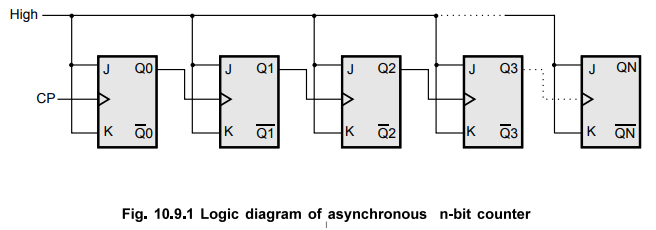
The
Fig. 10.9.1 shows the 4-bit asynchronous down counter using JK flip-flops.
Here, the clock signal is connected to the clock input of only first flip-flop.
This connection is same as asynchronous/ripple up counter. However, the clock
input of the remaining flip-flop is triggered by the Q output of the previous
stage.
 Listing
10.9.15 : VHDL description of an N-bit asynchronous down counter using generate
statement.
Listing
10.9.15 : VHDL description of an N-bit asynchronous down counter using generate
statement.
library
ieee;
use
ieee.std_logic_1164.all;
entity
asyn_ctr is
generic
(N : integer := 4); - This is a 4-bit counter.
port
( CP : in std_logic ;
Q,
Qbar : buffer std_logic_vector (N-l downto 0));
end
asyn_ctr;
architecture
asyn_ctr_gen of asyn_ctr is
component
JK_FF is
port(
II, 12, 13 : in std_logic;
Ol,
02 : buffer std_logic);
end
component;
for
ail: JK_FF use entity work. JKFF (FF);
signal
s : std_logic_vector (N downto 0);
begin
s
<= (Q & CP);
-
s is the concatenation of Q and CP. This concatenation is necessary to
-
specify the clock of each JK flip-flop in generic statement.
Gnlop
: for i in (N-l) downto 0 generate
G1
: JK_FF port map ('1', '1', s(i), Q(i), Qbar(i));
end
generate GnLop;
end
asyn_ctr_gen;
Ex.
10.9.3 : Structural description of an N-bit memory word using Generate.
This
single memory cell can be expanded to N-bit using the generate statement. This
is illustrated in listing 10.9.16.
Listing
10.9.16 : VHDL description of N-bit memory word using generate
library
ieee;
use
ieee.std_lo9ic_1164.all;
entity
memory_word is
generic
(N : integer := 8);
port
( D_in : in std_logic_vector (N downto 0);
Sel,
R_W : in std_logic;
D_out
: out std_logic_vector (N downto 0));
end
memoryword;
architecture
word_gen of memory_word is
component
memory_cell
port
( Sel, RW, Din : in std_logic;
O1
: buffer std_logic );
end
component;
for
all: memory cell use entity work.memory (mem_cell);
begin
G1
: for i in 0 to N generate
M
: memory_cell port map (sel, R_W, D_in(i), D_out(i));
end
generate;
end
word_gen;
Ex.
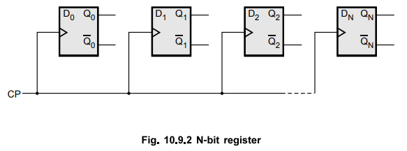
10.9.4 : Structural description of N-bit register.
The
group of flip-flops can be used to store a word, such a group is called
register. The Fig. 10.9.2 shows the N-bit register constructed with D
flip-flops. This register is called buffer register. Each D flip-flop is
triggered with a common clock pulse.
Listing
10.9.17 : VHDL description of N-bit register.
library
ieee;
use
ieee.stdlogicl 164.all;
entity
Regis is
generic
(N : integer : = 8); - 8-bit
register
port(D
: in std_logic_vector(N-l downto 0);
CP
: in std_logic;
Q,
Qbar : out std_logic_vector(N-l downto 0));
end
Regis;
architecture
register_nBit of Regis is
component
D_FF is
port(
I1, I2 : in std_logic;
Ol,
02 : buffer std_logic);
end
component ;
begin
build:
for i in 0 to N-l generate
for
ail: D_FF use entity work.DFF (FF);
begin
d
: D_FF port map(D(i),CP, Q(i), Qbar(i));
end
generate build;
end
register_nBit;
Ex.
10.9.5 : Structural description of N-bit shift register.
The
binary information (data) in a register can be moved from stage to stage within
the register or into or out of the register upon application of clock pulses.
This type of bit movement or shifting is essential for certain arithmetic and
logic operations used in microprocessors. This gives rise to a group of
registers called 'shift registers'. They are very important in applications
involving the storage and transfer of data in a digital system.
The
Fig. 10.9.3 shows the N-bit left shift register. Here, the data is shifted left
by one bit on receiving every clock pulse. Din is a serial input signal and
Dout is a data output signal.
![]()
Listing
10.9.18 : VHDL description of N-bit left shift register
library ieee;
use
ieee.std_logic_1164.all;
entity
Regis_Ls is
generic
(N : integer := 8); - 8-bit
register
port(Din
: in std_logic;
CP
: in std_logic;
Dout
: out std_logic;
Q,
Qbar : out std_logic_vector(N-l downto 0));
end
Regis_Ls;
architecture
register_nBit of Regis_Ls is
component
D_FF is
port(
I1, I2 : in std_logic;
O1,
O2 : buffer std_logic);
end
component ;
begin
build:
for i in 0 to N-l generate
for
all: D_FF use entity work.DFF (FF);
signal
D : std_logic_vector (N downto 0);
begin
D
< = (Q 8c Din);
d
: D_FF port map(D(i), CP, Q(i), Qbar(i));
end
generate build;
Dout
<= D(N);
end
register_nBit;
Review Questions
1. Explain the organization of the structural description with
the help of example.
2. Write the VHDL code to realize ai - hit parallel binary adder
with structural modelling and write the test bench to verify its functionality.
Digital Logic Circuits: Unit V: VHDL : Tag: : VHDL - Organization of Structuural Description
Related Topics
Related Subjects

Digital Logic Circuits
EE3302 3rd Semester EEE Dept | 2021 Regulation | 3rd Semester EEE Dept 2021 Regulation