Linear Integrated Circuits: Unit I: IC Fabrication
Oxidation in IC Fabrication
different techniques with diagram
The process in which a thin layer of silicon dioxide (SiO2) formed on a surface of silicon wafer using thermal growth technique is called oxidation
Oxidation
The
process in which a thin layer of silicon dioxide (SiO2) formed on a
surface of silicon wafer using thermal growth technique is called oxidation. In
the planar process it is essential to protect certain regions of surface of the
wafer so that the dopant atoms may be driven into other selective regions
during the processes such as diffusion or ion implantation. For such shielding
purpose, silicon dioxide (SiO2) is best suited. Some of the
important properties of SiO2 are as follows.
i)
It acts as mask or shield against implant or diffusion of dopant into silicon
wafer.
ii)
It provides surface passivation.
iii)
It acts as a component in MOS structures.
iv)
It provides electrical isolation between multilevel interconnected layers.
v)
The most commonly used silion dopants such as phosphorus, boron, arsenic and
antimony diffuse with difficulty in SiO2. In other words, all these
dopants have low diffusion coefficient in SiO2. Hence SiO2
acts as shield against all the above mentioned impurities.
Following
are the different techniques developed for forming oxide layers.
i)
Thermal oxidation.
ii)
Wet anodization or oxidation.
Iii
Vapour-phase technique (CVD).
iv)
Plasma anodization or oxidation.
Thermal
oxidation is the basic process in the fabrication of
semiconductor devices. When the interface between oxide and silicon requires a
low charge density level, this type of oxidation is preferred.
When
the oxide layer is required on the top of a metal layer such as in multilevel
metallization structure, the vapour phase technique i.e. chemical vapour
deposition (CVD) is used.
Plasma
oxidation is a low temperature vacuum process carried out in a pure oxygen
discharge. This process allows to grow high quality oxides on the surface of
silicon wafer as compared with other techniques. The plasma oxidation can grow
thick oxide layers at comparitively lower temperatures with higher growth rate.
The growth rate depends on temperature of substrate, plasma density and dopant
concentration in substrate.
1. Thermal Oxidation
The
oxidation processes is called thermal oxidation because to grow the oxide
layer, the temperature maintained is high.
The
selection of the oxidation technique depends upon the thickness and the oxide
properties required. For thin oxides with low charge density at interface, the
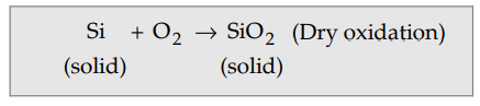
oxides are grown in dry oxygen. This is also called dry oxidation explained by
the reaction given below.
For
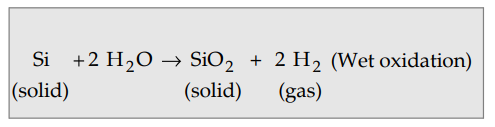
thick layers of oxides, steam or water vapour is used at high pressure for
oxidation. This is called wet oxidation. The chemical reaction for wet oxidation
is as follows.
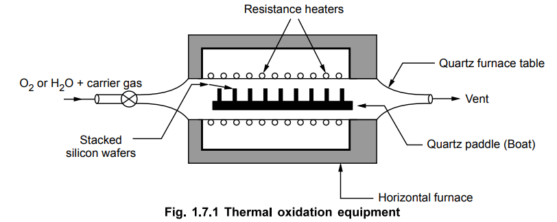
In
the most commonly used oxidation technique, the wafers are stacked vertically
in a slotted paddle or boat which is open ended. This is made up of quartz and
it is placed in quartz tube. This quartz tube is slowly passed through
resistance heated horizontal furnace. Typically the temperature maintained is
700 °C to 1200 °C. The oxidizing agent used may be dry oxygen or a mixture of
oxygen and water vapour. The schematic for the thermal oxidation equipment is as
shown in the Fig. 1.7.1.
Basically
an oxidation is high temperature process. Due to the oxidation process, the
layer departs from its original location. To overcome this undesired result,
the oxidation process is carried out at low temperatures. But this increases
the growth time. To overcome this, pressure is increased because an increase by
1 atm pressure, decreases temperature by 20 °C for same growth rate. Thus high
pressure oxidations with pressures upto 25 atm are used in the industrial
applications at the temperatures in the range of
Initially
the oxide growth formation rate is very fast and then gradually it slows down,
as oxygen atoms have to diffuse through the oxide to reach the interface
between silicon substrate and SiO2. As compared to dry oxidation process, wet
oxidation process is faster at a given temperature. Typically to grow 1 pm
thick oxide layer, dry oxidation process takes 2 hour 30 minutes, while wet
oxidation takes only 1 hour and 30 minutes. Eventhough the wet oxidation
process is time saving, it has a drawback of higher impurity contents of the
oxides. Generally MOS ICs require a very pure oxide for reliable performance.
For this purpose specially dry oxidation process is preferred.
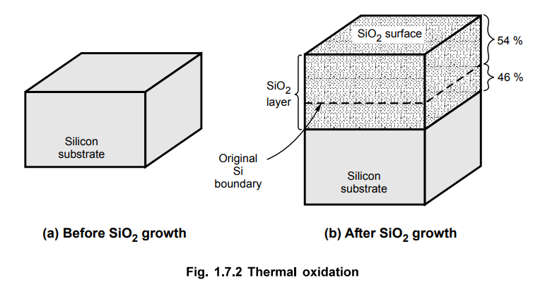
The
process is known as thermal oxidation because the oxide layer is formed on
silicon wafer using high temperatures. The silicon surface has very high
affinity for oxygen, an oxide layer rapidly forms when silicon is exposed to a
oxidising agent even at room temperature. During the oxidation process, the
Si-SiO2 interface pierces into the silicon substrate. It is observed
that after completion of oxidation process, the oxide of thickness d consumes
0.44 d thickness of silicon. This is illustrated in the Fig. 1.7.2.
Review Questions
1. Explain importance of SiO2 layer.
2. Describe the step of oxidation in IC Fabrication.
3. Write a note on different techniques of oxidation.
4. With the help of neat diagram, explain thermal oxidation
process. Write chemical reaction.
Linear Integrated Circuits: Unit I: IC Fabrication : Tag: : different techniques with diagram - Oxidation in IC Fabrication
Related Topics
Related Subjects

Linear Integrated Circuits
EE3402 Lic Operational Amplifiers 4th Semester EEE Dept | 2021 Regulation | 4th Semester EEE Dept 2021 Regulation