Digital Logic Circuits: Unit II: Combinational Circuits
Parallel Adder
Block diagram, Working Principle | Combinational Circuits
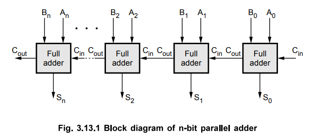
• We have seen, a single full-adder is capable of adding two one-bit numbers and an input carry. In order to add binary numbers with more than one bit, additional full-adders must be employed.
Parallel Adder
•
We have seen, a single full-adder is capable of adding two one-bit numbers and
an input carry. In order to add binary numbers with more than one bit,
additional full-adders must be employed. A n-bit, parallel adder can be
constructed using number of full adder circuits connected in parallel. Fig.
3.13.1 shows the block diagram of n-bit parallel adder using number of
full-adder circuits connected in cascade, i.e. the carry output of each adder
is connected to the carry input of the next higher-order adder.
•
It should be noted that either a half-adder can be used for the least
significant position or the carry input of a full-adder is made 0 because there
is no carry into the least significant bit position.
Ex.
3.13.1 Design a 4-bit parallel adder using full-adders.
Sol.
:
Fig. 3.13.2 shows the block diagram for 4-bit adder. Here, for least
significant position, carry input of full-adder is made 0.

Review Questions
1. What is parallel adder ?
2. Draw and explain the working of 4-bit parallel adder.
3. Design a 4-bit binary ripple carry adder with full adders and
discuss its operation.
Digital Logic Circuits: Unit II: Combinational Circuits : Tag: : Block diagram, Working Principle | Combinational Circuits - Parallel Adder
Related Topics
Related Subjects

Digital Logic Circuits
EE3302 3rd Semester EEE Dept | 2021 Regulation | 3rd Semester EEE Dept 2021 Regulation