Linear Integrated Circuits: Unit I: IC Fabrication
Realization of Active and Passive Devices in Integrated Circuits
1. Monolithic Transistor 2. Planar p-n Junction Diode Fabrication 3. Integrated Resistors 4. Integrated capacitors 5. Integrated inductors 6. integrated FETs
Realization of Active and Passive Devices in Integrated Circuits
May-04,06,07,08,10,12,14,15,16,18,
Dec.-03,05,07,08,09,11,12,14,16,17
In
this section, we shall study how to realize active and passive devices such as
transistors, diodes, resistors, capacitors and inductors etc. in integrated
circuits.
1. Monolithic Transistor
The
cross-sectional view of an integrated monolithic transistor and discrete planar
transistor are as shown in the Fig. 1.14.1 (a) and (b) respectively.

The main difference between monolithic integrated transistor and discrete planar transistor is that collector contact in monolithic integrated transistor is at top, while in the discrete planar transistor it is at bottom. Because of this the collector series resistance of the collector current path increases. This effectively increases the collector to emitter voltage VCE(sat) of the device. Also in monolithic integrated transistor as substrate is held at negative potential, additional parasitic capacitance appears between collector and substrate.
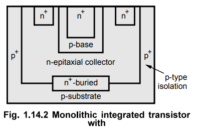
To
overcome the increase in collector series resistance, buried n+ layer is
incorporated by using additional process step. The buried layer can be
processed with heavily doped n+ region in between p-type substrate
and n-type epitaxial collector. The advantage of burned n+ layer is
that it provides low resistivity current path as shown in the Fig. 1.14.2. The
buried n+ layer shunts n-epitaxial collector layer effectively decreasing
resistance.
a.
p-n-p Transistor
There
are different ways of fabricating p-n-p transistor in integrated circuits. The
important means of integrating p-n-p transistor are (i) vertical p-n-p, (ii)
lateral p-n-p and (iii) triple diffused p-n-p.
In
vertical p-n-p transistor, the p type substrate is used as p-type collector
while the n-epitaxial layer is used as base. Obviously the next diffusion layer
of p-type is used as an emitter. This type of p-n-p is called as substrate
p-n-p transistor. The main drawback is that collector has to be held at a fixed
negative potential.
The
lateral p-n-p transistor is formed without any additional process. The p-n-p
transistor is formed simultaneously with n-p-n transistor. Here n-epitaxial
layer is used as base simultaneously two p-regions are diffused to form emitter
and corrector ring as shown in the Fig. 1.14.3.

If
an extra p-type diffusion is added after n-diffusion then we can get p-n-p
transistor starting for standard n-p-n transistor. The p-n-p transistor thus
obtained is called triple diffused p-n-p transistor. This type of transistor is
fabricated only if there is a special need because of complicated process
calculations and increase in cost due to addition in fabrication process.
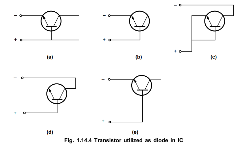
2. Planar p-n Junction Diode Fabrication
Diodes are used extensively in the integrated circuits, for various applications such as digital applications. Note that in the integrated circuits, a p-n junction diode is formed from the bipolar transistor. Generally any two terminals of the transistor are connected together to get one terminal of diode, while the remaining terminal of the transistor serves as the second terminal of diode. Different transistor connections to utilize it as a diode are as shown in the Fig. 1.14.4.
Depending
upon desired circuit performance and application, diode connection is selected.
The diode represented in the Fig. 1.14.4 (a) is used in digital circuits for
high speed applications because of its lowest storage time and lowest forward
voltage drop. The diodes represented in the Fig. 1.14.4 (b) and (e) are used as
stored charged devices. The diodes represented in the Fig. 1.14.4 (c) and (d)
have highest breakdown voltage.
Fabrication
of a planar p-n junction diode is illustrated in the Fig. 1.14.5.
The
starting material for the planar p-n junction diode is n+ substrate which is
grown by using Czochralski growing process. The substrate is about 150 µm
thick.

Using
epitaxial growth process, a layer of n-type silicon is deposited on the substrate.
The layer is about 1 to 5 µm thick.
Using
oxidation process, silicon dioxide (SiO2) is deposited.
The
surface is then coated with positive photoresist.

Appropriate
mask is placed over the positive photoresist layer. It is properly aligned and
then exposed to the ultraviolet light.

Then
the mask is removed and photoresist is removed. Using etching process, only
silicon dioxide layer under the exposed resist is etched.

Then
to form p-region, boron is diffused using ion-implantation process.

Boron
diffuses in silicon easily, but not in SiO2. The resulting p-region
is defined by the oxide opening. The width of p-region is slightly greater than
the oxide opening because of lateral doping during dopant diffusion.

Using
Metallization, thin film of aluminium is deposited.

Then
the metallized area is covered with photoresist. Another mask is placed over
photoresist which ensures areas of metal to be preserved.

The
wafer is then etched to remove unwanted metal. The photoresist is then
dissolved. The contact metal is deposited on the back surface and using heat treatment
ohmic contacts are made.

3. Integrated Resistors
In
integrate circuit design, the importance is given to the maximum usage of
transistors. For example digital CMOS, nMOS and GaAs circuits are fabricated
entirely with transistors and diodes. The resistors are grouped into two groups
; one formed within monolithic IC and other composed of film resistors.
The
monolithic IC resistors consist suitably dimensioned layers which would form
part of the transistor normally. Obviously the resistivity of such layers is
determined from transistor characteristics.
If
the resistor is formed in one of the isolated regions of epitaxial layer during
base or emitter diffusion, then it is called diffused resistor. It is very
economical process as no additional steps in fabrication are needed. But the
limitation of the diffused resistor is that the range of the value of
resistance is very small.
For
larger value of resistor, the larger area of silicon is required. Hence the
high value resistances are realized by using pinch resistor as shown in the
Fig. 1.14.6.

The
amount of silicon required for the value of resistor beyond 100 kQ is
relatively low. The accuracy of such resistors is poor. For high value
resistors accuracy is not important point to take care. It consists of p base
layer constricted by an n+ emitter layer, leading to an effective thickness
equal to base thickness of a npn transistor.
As
we have already studied that the resistance can be realized by using a defined
volume of semiconductor region. Consider a sheet of material with length L and
width W as shown in the Fig. 1.14.7. Let t be the thickness and p be the
uniform resistivity.
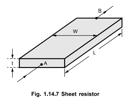
The
resistance R between layers A and B is given by
A
= ρ L / A = ρ L / t W ... (1.14.1)
For
square surface area, W = L, then the resistance of the material is given by
Rs
= ρ L / (t L) = ρ / t ... (1.14.2)
Thus
rearranging equation (1.14.1) using equation (1.14.2), we can write
R
= Rs (L / W)
Here
ratio L/W is called aspect ratio. Thus using this technique base resistor in
the
range
20 Ω to 300 k Ω can be fabricated. Similarly the resistance of the
emitter diffusion can be fabricated as sheet resistor but the range of
resistance is only 10 to 1 k Ω.
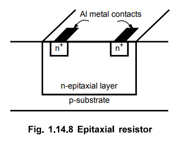
By
using n-epitaxial collector layer, the large value resistances than base and
emitter diffusion can be achieved. Such resistors are called epitaxial
resistors as shown in the Fig. 1.14.8.
4. Integrated capacitors
The
common parallel plate capacitor structures are as shown in the Fig. 1.14.9.

In
most widely used type shown in Fig. 1.14.9 (a), the two polysilicon plates are
seperated by silicon dioxide (SiO2). Here the lower plate rests on
the top of the substrate.
The
capacitor shown in Fig. 1.14.9 (b) is MOS capacitor. It consists a implanted or
diffused heavily doped layer within substrate while a polysilicon or metal
plate on the top of a thin oxide layer. For MOS capacitors, generally gate
oxide is used with no extra processing step.
5. Integrated inductors
In
ICs, inductors, transformers and chockes are not integrated because of
bulkiness. The inductors can be fabricated on a chip in the form of a thin film
spirals by successively depositing the conducting patterns. But using
fabricated inductor, a very small value of inductor is possible which is of the
order of few nano-henries. But the practical approach is not to integrate
inductors. The inductors are simulated on a chip with the help of R-C networks
or some other type of a network. In case of RF and IF circuits, the use of
inductor is unavoidable. Under such conditions, inductors are used externally
with the integrated circuit.
6. integrated FETs
In
general the field effect transistors are of two types namely
i)
Junction Field Effect Transistor (JFET)
ii)
Metal Oxide Semiconductor Field Effect Transistor (MOSFET)
a.
integrated JFET
The
basic processes used for the fabrication of JFET are exactly similar to those
used in the fabrication of BJT. The JFETs are further classified as n-channel
JFET and p-channel JFET. The development of n-channel JFET is as shown in the
Fig. 1.14.10.

The
JFET, the epitaxial layer is used as n-channel. The p+ gate is
formed in n-type channel by ion-implantation or diffusion process. While good
ohmic contacts are achieved by using n+ diffusion layers below
b.
Integrated MOSFETs
MOSFETs
are classified as follows
i)
Enhancement mode MOSFET
ii)
Depletion mode MOSFET
In
MOSFETs gate terminal is isolated from the FET channel by silicon dioxide
insulating layer. As the layer is insulating type, it provides very high input
resistance. In providing superior barrier for impurities penetrating SiO2
layer, silicon nitride (Si3N4) is sandwiched between two
silion dioxide (SiO2) layers. This helps in increasing overall
dielectric constant.
The
n-channel MOSFET of enhancement and depletion mode are as shown in the Fig.
1.14.11 (a) and (b) respectively.

In
the enhancement mode, MOSFET is in OFF state when gate-source bias is zero,
while MOSFET turns ON by positive gate source voltage. In depletion mode,
because of n-implanted channel conduction is possible in ON state for zero
gate-source voltage. While negative gate source voltage is required to turn it
OFF.
c.
Integrated CMOSs
When
n-channel MOSFET and p-channel MOSFET both are integrated on same chip, the
device is termed as complementary CMOS. In CMOS fabrication, n-type well is
diffused in p-type substrate. Also p-channel MOSFET is fabricated within this
n-well. Basically this n-well forms substrate for p-channel MOSFET. In the
fabrication of p-channel MOSFET two additional steps are required as compared
to n-channel MOSFET fabrication. The additional steps are formation of n-well
and ion-implantation of p-type source and drain regions. The cross section of
CMOS IC is as shown in the Fig. 1.14.12.

Review Questions
1. What is thin and thick film technology ? Explain various
methods used for deposition of thin film technology.
2. Explain the various methods of fabricating diodes and
transistors in a monolithic integrated circuits.
3. Can inductors be fabricated in IC ? Explain.
4. Discuss the various methods used for fabricating IC resistors
and compare their performance.
May-06, 10, Marks 8
5. What are the different ways by which the diode structures can
be realized in IC ?
6. With neat sketches describe the various types of integrated
resistors.
7. Discuss the different ways to fabricate diodes.
Dec.-07, 08, Marks 8; May-08, 13, Marks 8
8. Sketch a MOS capacitor and explain the difference between MOS
capacitor and junction capacitor.
Dec.-07, Marks 10; Dec.-11, Marks 8; Dec.-14, Marks 10
9. Discuss the self-aligning property of a polysilicon gate
MOSFET.
10. How a PN junction diode is formed in IC fabrication ?
May-08, Marks 6
11. How are resistors and capacitors fabricated in monolithic
technology? Discuss.
Dec.-09, 14, Marks 16
12. Explain the basic processes used in silicon planar
technology with neat diagram.
May-10, Dec.-17, Marks 16
13. Explain in detail the fabrication process of passive
component in integrated circuits.
14. Elaborate the fabrication of MOS ICs with suitable diagram.
15. Explain the fabrication of n-channel JFET with necessary diagrams.
May-12, 18, Marks 16 May-18, Marks 13
16. Write a note on recent fabrication methods of FET for
industrial applications.
Dec.-16, Marks 15
Linear Integrated Circuits: Unit I: IC Fabrication : Tag: : - Realization of Active and Passive Devices in Integrated Circuits
Related Topics
Related Subjects

Linear Integrated Circuits
EE3402 Lic Operational Amplifiers 4th Semester EEE Dept | 2021 Regulation | 4th Semester EEE Dept 2021 Regulation