Linear Integrated Circuits: Unit I: IC Fabrication
Realization of Monolithic Integrated Circuit
IC Fabrication
Along with transistors, diodes, resistors and capacitors are also integrated over a single silicon wafer which is called monolithic IC.
Realization of Monolithic Integrated Circuit
May-04,05,07,10,11,15,17,18,
Dec.-06,07,08,10,12,14,15,17
After
the discussion of the basic fabrication processes let us now consider how
circuit is converted into monolithic integrated circuit. The key element in the
IC is the transistor. Along with transistors, diodes, resistors and capacitors
are also integrated over a single silicon wafer which is called monolithic IC.
The interrelationship between various processes steps in the fabrication of IC
is illustrated in the Fig. 1.15.1.

The
starting material for the IC fabrication is the polished silicon wafer with a
specific orientation and resistivity. The formation of oxide films using
thermal oxidation and deposition of polysilicon, dielectric for isolation and
metal films for interconnections are included in film deposition. Then it is
followed by the lithography or ion implantation process. Then it is subjected
to the etching process. The final IC is made by sequentially transfering the
patterns from set of masks onto the surface of a wafer.
After
processing, the wafer consists thousands of rectangular chips which all are
identical. Then chips are separated by using laser cutting. The chips are
tested electrically. The faulty chips are marked and removed from the batch,
while the good ICs are packaged to provide proper termal, electrical,
interconnection enviornment for different electric applications.
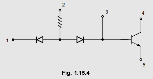
Consider
a simple circuit as shown in Fig. 1.15.2.

For
the illustration of complete fabrication process of the monolithic IC.
A.
Preparation of wafer
The
starting material for the integrated circuit is p-type silicon which is called
substrate. Typically the thickness of the wafer ranges in between 400 µm to 500
µm. The diameter of the silicon wafer ranges between 100 mm to 200 mm. For the
acceptor concentration of 1.4 ×10¹⁵ atoms/cm3 the
resistivity is 10 - 15 Ω cm. Refer Fig. 1.15.3 (a).

B.
Epitaxial growth
Generally
the doping types of the substrate and the epitaxial layer are opposite to
provide isolation. Thus n-type epitaxial layer is grown on p-type subtrate
which has resistivity of the order 1-2 Ωcm. The epitaxial layer is useful as
other components are fabricated within this layer. This layer may act as an
element of diode, diffused capacitor of collector of transistor. Refer Fig.
1.15.3 (b).

C.
Oxidation
After
the growth of an epitaxial layer, SiO2 layer is grown on the n-epitaxial
layer. This oxide layer is grown by using thermal oxidation method. The
thickness of the SiO2 layer is smaller as compared to previous
layers. Typically it ranges between 0.05 to 2 µm Refer Fig. 1.15.3 (c).

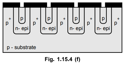
D.
Lithographic process
Then
the wafer is coated with negative photoresist. To isolated the four components
of the circuit, p+ type layer is diffused. For this a opening has to be made
using the proper mask. So proper mask is kept on a wafer and then u.v. light is
passed. After that it is photoetched to get a wafer with openings for isolation
diffusion. Refer Fig. 1.15.3 (d). Note that we will have to use this process
frequently with different pattern of the mask.

E.
Isolation diffusion using p-n junction isolation technique
After
the lithographic process, from the openings from where SiO2 is etched out,
heavy doping of p-type is diffused for very long interval such that the
impurities reach p-substrate penetrating n-type epitaxial layer. Thus we get for
isolation island for four components. Generally the concentration of ecceptor
atoms between isolation island is kept higher than p-substrate which ensures
perfect electrical isolation. Refer Fig. 1.15.3 (e).

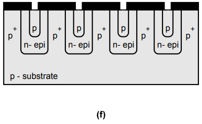
F.
Base diffusion
After
isolation diffusion once again a layer of SiO2 is grown over a wafer and then
using again photo lithographic technique different pattern is marked on wafer
to have opening for the diffusion of p-type impurity such as boron. The
impurity diffusion depth is controlled so that it can not penetrate epitaxial
layer to reach p-substrate. Refer Fig. 1.15.3 (f). This serves as base of
transistor, anode of diode etc.
G.
Emitter diffusion
After
base diffusion, another set of windows is required to diffuse n-type impurity
for the capacitor, diode and transistor. Hence again SiO2 layer is
grown on the wafer and using diffemet mask, new set of windows is opened using
photo lithographic process. Then through the new set of windows, n-type impurity
e.g. phosphorus is diffused which forms emitter of transistor and cathode of
diode.
The
windows are etched by using wet etching technique. Refer Fig. 1.15.3 (g).

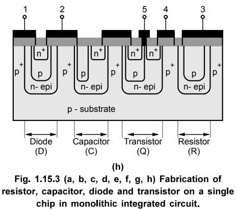
H.
Metallization
The
final step in the process of IC fabrication is making interconnection using
aluminium metal. For this again wafer is grown with SiO2 layer and using new
photomask, new set of windows is opened at points from where terminals are to
be brought out. After the interconnections are made IC is subjected to the
packaging processes. Refer Fig. 1.15.3 (h).
Example
1.15.1 With the help of neat diagram explain the steps involved in the
fabrication of the circuit shown in the Fig. 1.15.4 using IC technology.
May-04,
Marks 18
Solution :
A.
Preparation of wafer
The
starting material for the integrated circuit is p-type silicon which is called
substrate. Typically the thickness of the wafer ranges in between 400 μm to 500
μm. The diameter of the silicon wafer ranges between 100 mm to 200 mm. For the
acceptor concentration of 1.4 × 10¹⁵ atoms/cm3 the
resistivity is 10-15 Ωcm.

B. Epitaxial growth
Generally
the doping types of the substrate and the epitaxial layer are opposite to
provide isolation. Thus n-type epitaxial layer is grown on p-type subtrate which
has resistivity of the order 1-2 Ωcm. The epitaxial layer is useful as other
components are fabricated within this layer. This layer may act as an element
of diode, diffused capacitor of collector of transistor. Refer Fig. 1.15.4 (b).

C.
Oxidation
After
the growth of an epitaxial layer, SiO2 layer is grown on the
n-epitaxial layer. This oxide layer is grown by using thermal oxidation method.
The thickness of the SiO2 layer is smaller as compared to previous
layers. Typically it ranges between 0.05 µm to 2 µm Refer Fig. 1.15.4 (c).

D.
Lithographic process
Then
the wafer is coated with negative photoresist. To isolate the four components
of the circuit, p+ type layer is diffused. For this a opening has to be made
using the proper mask. So proper mask is kept on a wafer and then u.v. light is
passed. After that it is photoetched to get a wafer with openings for isolation
diffusion. Refer Fig. 1.15.4 (d). Note that we will have to use this process
frequently with different pattern of the mask.

E.
Isolation diffusion using p-n junction isolation technique
After
the lithographic process, from the openings from where SiO2 is
etched out, heavy doping of p-type is diffused for very long interval such that
the impurities reach p-substrate penetrating n-type epitaxial layer. Thus we
get for isolation island for four components. Generally the concentration of
acceptor atoms between isolation island is kept higher than p-substrate which
ensures perfect electrical isolation. Refer Fig. 1.15.4 (e)

F.
Base diffusion
After
isolation diffusion once again a layer of SiO2 is grown over a wafer
and then using again photolithographic technique different pattern is marked on
wafer to have opening for the diffusion of p-type impurity such as boron. The
impurity diffusion depth is controlled so that it cannot penetrate epitaxial
layer to reach p-substrate. Refer Fig. 1.15.4 (f).
This
serves as base of transistor, anode of diode etc.
G.
Emitter diffusion
After
base diffusion, another set of windows is required to diffuse n-type impurity
for the capacitor, diode and transistor. Hence again SiO2 layer is
grown on the wafer and using different mask, new set of windows is opened using
photolithographic process. Then through the new set of windows, n-type impurity
e.g. phosphorus is diffused which forms emitter of transistor and cathode of
diode
The
windows are etched by using wet etching technique. Refer Fig. 1.15.4 (g).

H.
Metallization
The
final step in the process of IC fabrication is making interconnection using
aluminium metal. For this, again wafer is grown with SiO2 layer and using new
photomask, new set of windows is opened at points from where terminals are to
be brought out.
After
the interconnections are made IC is subjected to the packaging processes. Refer
Fig. 1.15.4 (h).

Review Questions
1. Briefly explain various processes involved in fabrication of
monolithic IC which integrates diode, capacitance and FET.
May-15, Dec.-17, Marks 16
2. Explain the basic processes used in the fabrication of
monolithics IC.
May-04, 05, 11, 17, Dec.-12, Marks 16; May-07, Marks 8; Dec.-08,
17, Marks 12
3. Explain the basic processes used in silicon planar technology
with neat diagram.
May-10, 18, Marks 16
4. With respect to the BJT based circuit shown in Fig. 1.15.5,
explain the various steps to implement the circuit into a monolithic IC.
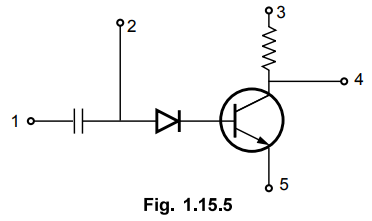
Dec.10, Marks 16
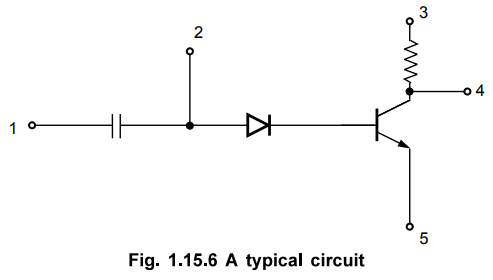
5. Draw the cross-sectional view of the typical fabricated
circuit given in Fig.1.15.6 and explain the fundamentals of monolithic IC technology.
Dec.-06, Marks 10
6. With circuit diagram explain the steps involved in the
fabrication of the circuit shown below using IC technology
May-17, Marks 13

7. Explain the fabrication process involved in the given circuit
diagram. (Refer Fig. 1.15.8)
Dec.-14, Marks 10

8. Explain the various steps involved in fabrication of a
typical transistor into monolithic ICs.
Dec.-15, Marks 16
Linear Integrated Circuits: Unit I: IC Fabrication : Tag: : IC Fabrication - Realization of Monolithic Integrated Circuit
Related Topics
Related Subjects

Linear Integrated Circuits
EE3402 Lic Operational Amplifiers 4th Semester EEE Dept | 2021 Regulation | 4th Semester EEE Dept 2021 Regulation