Digital Logic Circuits: Unit V: VHDL
RTL Design using VHDL with example
• To show how an RTL design is described in VHDL and to clarify the concepts involved, we will design a four-input adder. This design will also demonstrate how to create packages of components that can be re-used.
RTL Design Example
AU
: May-12, Dec.-15
•
To show how an RTL design is described in VHDL and to clarify the concepts
involved, we will design a four-input adder. This design will also demonstrate
how to create packages of components that can be re-used.
•
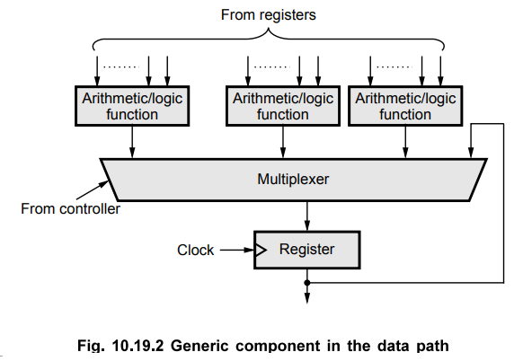
The datapath shown in Fig. 10.20.1 can load the register at the start of each
clock cycle with one of : zero, the current value of the register, or the stun
of the register and one of the four inputs. It includes one 8-bit register, an
8-bit adder and a multiplexer that selects one of the four possible inputs as
the value to be added to the current value of the register.

•
The first design unit is a package that defines a new type, num, for eight-bit
unsigned numbers and an enumerated type, states, with six possible values, nums
are defined as a subtype of the unsigned type.
—
RTL design of 4-input summer
—
subtype used in design
library
ieee ;
use
ieee.std_logic_1164.
use
ieee.std_logic_arith.all;
package
summer is
subtype
num is unsigned (7 downto 0) ;
type
states is ( clr, add_a, add_b, add_c,
add_d,
hold) ;
end
summer ;
•
The first entity defines the datapath. In this case the four numbers to be
added are available as inputs to the entity and there is one output for the
current sum. The inputs to the datapath from the controller are a 2-bit selector
for the multiplexer and two control signals to load or clear (set to 0) the
register.
—
datapath
library
ieee ;
use
ieee.std_logic_1164.
use
ieee.std_logic_arith.all ;
use
work.summer.all;
entity
datapath is
port
( a, b, c, d : in num ;
sum
: out num ;
sel:
in std_logic_vector (1 downto 0) ;
load,
clear, elk : in std_logic
);
end
datapath ;
architecture
rtl of datapath is
signal
mux_out, sum_reg, next_sum_reg : num ;
constant
sum_zero : num :=
conv_unsigned(0,next_sum_reg’length)
; begin
—
mux to select input to add
with
sel select mux_out < =
a
when “00",
b
when “01",
c
when “10",
d
when others ;
—
mux to select register input
next
sum reg < =
sum_reg
+ muxout when load = T’ else
sum_zero
when clear = 1' else
sum_reg
;
—
register sum
process(clk)
begin
if
elk'event and elk = 1' then
sum_reg
< = next_sum_reg ;
end
if;
end
process ;
—
entity output is register output
sum
<= sum_reg ;
end
rtl;
•
The RTL design's controller is a sequential circuit whose outputs control the
multiplexers in the datapath. The controller's inputs are signals that control
the controller's state transitions. In this case the only input is an update
signal that tells our device to recompute the sum when one or more of the
inputs changes.
•
This particular state machine will remain in the "hold" state until
the update signal is true. It then sequences through the other five states and
then stops at the hold state again. The other five states are used to clear the
register and to add the four inputs to the current value of the register.
—
controller library ieee ;
use
ieee.std_logic_1164.all;
use
work.summer.all;
entity
controller is
port
( update : in std_logic ;
sel
: out std_logic_vector (1 downto 0) ;
load,
clear : out std_logic ;
clk
: in std_logic
);
end
controller ;
architecture
rtl of controller is
signal
s, holdns, ns : states ;
signal
tmp : std_logic_vector (3 downto 0);
begin
—
select next state
with
s select ns < =
add_a
when clr,
add_b
when add_a,
add_c
when add_b,
add_d
when add_c,
hold
when add_d,
holdns
when others ; — hold
—
next state if in hold state
holdns
< =
clr
when update = T’ else
hold
;
—
state register
process(clk)
begin
if
elk’event and elk = ’I’ then
s
< = ns ;
end
if;
end
process ;
—
controller outputs
with
s select sel < =
“00"
when add_a,
“01"
when add_b,
“10"
when add_c,
“11"
when others ;
load
< = ’0’ when s = clr or s = hold else 1’ ;
clear
<= ’I’ when s = clr else ’0’ ;
end
rtl;
•
The next section of code is an example of how the datapath and the controller
entities can be placed in a package, summer_components, as components. In
practice the datapath and controller component declarations would probably have
been placed in the top-level architecture since they are not likely to be
re-used in other designs.
—
package for datapath and controller
library
ieee ;
use
ieee.std_logic_1164.all;
use
work.summer.all;
package
summer_components is
component
datapath
port
( a, b, c, d : in num ;
sum
: out num ;
sel:
in std_logic_vector (1 downto 0) ;
load,
clear, clk : in std_logic
);
end
component ;
component
controller
port
( update : in std_logic ;
sel:
out std_logic_vector (1 downto 0) ;
load,
clear: out std_logic ; clk : in std_logic
);
end
component;
end
summer_components ;
•
The top-level summer entity instantiates the two components and interconnects
them.
—
summer
library
ieee ;
use
ieee.std_logic_1164.all;
use
ieee.std_logic_arith.all;
use
work.summer.all;
use
work.summer_components.all;
entity
summer is port ( a, b, c, d : in num ;
sum
: out num ; update, elk : in std_logic ) ;
end
summer ;
architecture
rtl of summer is
signal
sel: std_logic_vector (1 downto 0) ;
signal
load, clear : stdlogic ;
—
other declarations (e.g. components) here
begin
dl:
datapath port map ( a, b, c, d, sum, sel, load, clear, clk ) ;
cl:
controller port map ( update, sel, load, clear, clk );
end
rtl;
•
The result of the synthesizing the datapath is :
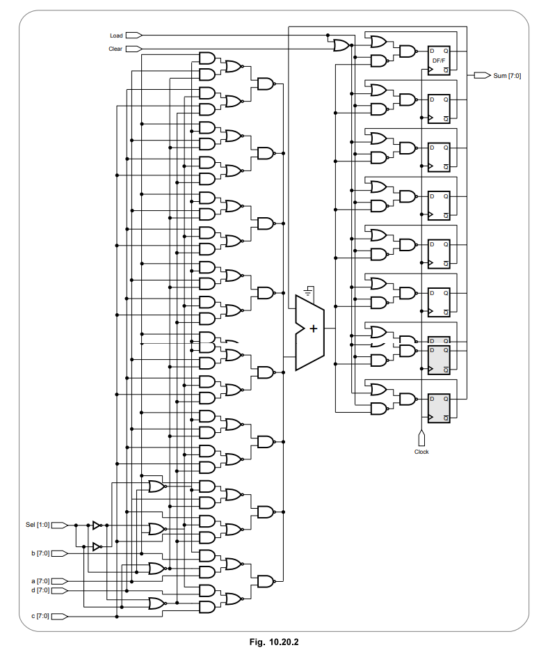
•
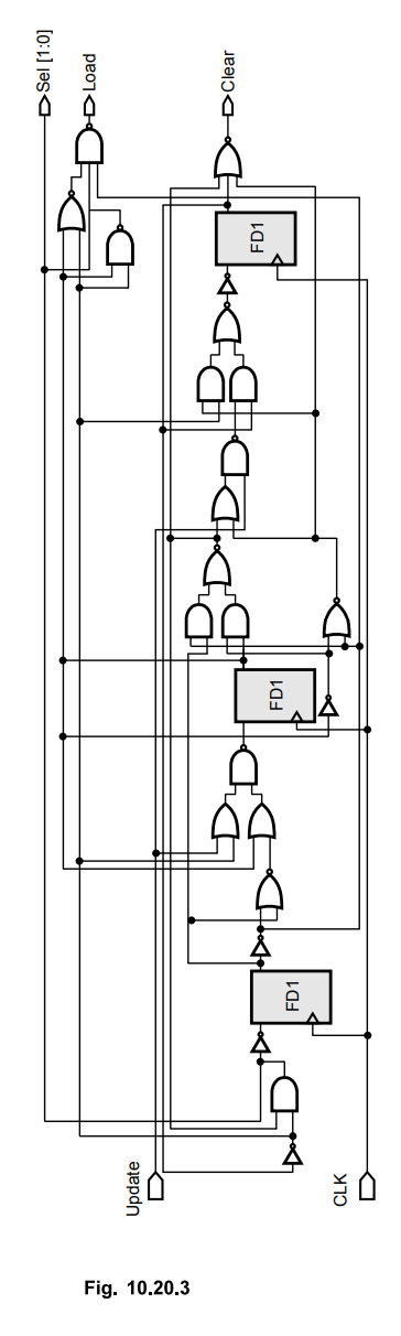
The register flip-flops are at the upper right, the adder is in the middle and
the input multiplexer is at the lower left. The result of the synthesizing the
controller is :
Review Question
1. Explain RTL design using VHDL with the help of example.
AU : Dec.-15, May-12, Marks 16
Digital Logic Circuits: Unit V: VHDL : Tag: : - RTL Design using VHDL with example
Related Topics
Related Subjects

Digital Logic Circuits
EE3302 3rd Semester EEE Dept | 2021 Regulation | 3rd Semester EEE Dept 2021 Regulation