Digital Logic Circuits: Unit V: VHDL
Structure of Data Flow Description
VHDL
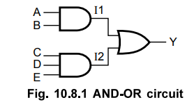
The circuit is an AND-OR circuit in which signals A, B, C, D and E are input signals, signal Y is an output signal and signals II and 12 are intermediate signals.
Structure of Data Flow Description
AU
: Dec.-12, 16
•
The listing 10.8.1 shows the HDL code for the circuit shown in the Fig. 10.8.1.
The circuit is an AND-OR circuit in which signals A, B, C, D and E are input
signals, signal Y is an output signal and signals II and 12 are intermediate
signals.
Listing
10.8.1 : VHDL code for AND-OR circuit
VHDL
AND-OR Circuit Description.
entity
AND_OR is
port
(A, B, C, D, E : in bit;
Y
: out bit);
end;
architecture
digital_ckt of AND-OR is
signal
I1, I2;
begin
stl
: I1 < = A and B after 10ns;
st2
:I2 < = C and D and E after 10ns;
st3
: Y < = Il or 12 after 20ns;
end
digital_ckt;
1. Signal Declaration and Assignment Statement
•
Here, input and output signals are declared in the entity as ports. However,
the intermediate signals (Il and 12 in the listing 10.8.1) are declared using
the predefined word signal in the architecture. A signal assignment operator
<= is used in VHDL to assign a value to the left-hand side of a
signal-assignment statement. The left-hand side of the statement should be
declared as a signal. The right-hand side can be a signal, a variable or a
constant.
2. Assigning a Delay Time to Signal Assignment Statement
•
The execution of assignment statement is done in two phases : calculation and
assignment. Consider the listing 10.8.1 and the simulation waveform shown in
the Fig. 10.8.2.

Calculation
: The
value of II is calculated using the current values of A and B at time TO. This
value is (1 and 0) = 0 in VHDL.
Assignment
: The
calculated value is not immediately assigned to II; however it is assigned to
II after a time delay of 10 ns. The delay time can be implicitly or explicitly
specified. In our case, we have assumed propagation delay of each gate as 10 ns
and hence we have explicitly specified time delay equal to 10 ns.
The
change in the II at T = 110 ns constitute an event in signal assignment
statement st3 and this causes execution of st3. For statement st3, at T = 110
ns, 12 = 0 and II = 0 and hence the calculated new value of Y at T = 110 ns is
(Il or 12) = 0. This change in value for Y from 1 to 0 is assigned to Y after
10 ns - that is, at T1 = 110 + 10 = 120 ns.
Important
points
•
To assign a delay time to a signal assignment statement, we use the predefined
word after (delay time) in VHDL.
•
In VHDL we specify delay in time units such as nsec, msec, sec etc.
3. Concurrent Signal Assignment Statements
•
Concurrent statements are order-independent and asynchronous. The most
important concurrent statement is the process declaration. Other concurrent
statements are the concurrent signal assignment statement : conditional signal assignment (WHEN-ELSE) and
selected signal assignment (WITH-SELECT-WHEN), the block statement, the
concurrent assert statement, the concurrent procedure call statement, the
component instantiation statement, and the generate statement. Let us see
examples and concurrent statements.
a.
Simple Assignment Statements
• A logic or arithmetic expression is called a
simple assignment statement.
•
For example :
f
<= X AND Y;
b.
Selected Signal Assignment
•
A selected signal assignment allows a signal to be assigned one of multiple
values, based on a selection criterion. Let us see the selected signal
assignment used in 2 to 1 multiplexer as an example. Assume that WO, W1 and S
are the inputs of multiplexer and f is the output. The selected signal
assignment begins with the keyword WITH, which specifies that S is to be used
for the selection criterion, as shown below. The two WHEN clauses state that f
is assigned the value of WO when S = 0; otherwise, f is assigned the value of
Wl.
WITH
S SELECT
f
< = WO WHEN 'O'
W1WHEN
OTHERS;
c.
Conditional Signal Assignment
•
It is similar to selected signal assignment. It allows a signal to be set to
one of several values. For 2 to 1 multiplexer, the conditional signal
assignment is as follows.
f
< = WO WHEN S = 'O' ELSE W1;
•
The common property of all the above statements is that the ordering of the
statements does not affect the meaning of the code. Hence, these statements are
called as 'the concurrent assignment statements'.
•
Hardware is not always a sequential circuit. There are many circuits which generate
output signal in parallel. To model such hardware we need concurrent
statements. The VHDL support concurrent statements. When statements are concurrent,
they execute in parallel. Concurrent signal assignment statement produces
multiple drivers, e.g. C <=A
•
Multiple Drivers
C
<= A AND B;
C
<= D AND E;
•
Drawback of concurrent statements is, it provides multiple drivers for a single
output. So to solve this problem you have to resolve the output. User written
resolution function defines it. The value of each driver is an input to the
resolution function and, based on the computation performed within resolution
function, the value returned from this function becomes the resolved value for
the signal.
Let
us see different types of concurrent statements.
WHEN
Statement
D
<= A WHEN SEL_A = "0" ELSE
B
WHEN SEL_B = "1" ELSE C;
•
In this concurrent statement whenever an event is occurred on signal used in
condition, the conditional signal assignment statement is executed.
WITH
SELECT
Syntax
WITH
expression SELECT
Target
< = Expressionl WHEN choicel
Expression2
WHEN choice2
Expressionn
WHEN choicen
•
It evaluates each choice expression and compares the value with each choice.
The selected signal assignment statement selects different values for target
signal based on the value of select expression. The semantics of a selected
signal assignment statement is, whenever an event occurs on a signal in the
select expression or on the expressions, the statement is executed. Based on
the value of the select expression that matches the choice value specified, the value of the corresponding
expression is scheduled to be assigned to the target signal. Note that the
choices are not evaluated in sequence. An "others" choice may cover
values not covered explicitly.
WITH
SELECT
WITH
sel_a SELECT
op
< = a WHEN "00",
b
WHEN "01",
c
WHEN "10"
0
WHEN OTHERS;
4. Comparison between Concurrent and Sequential Statement

5. Constant Declaration and Assignment
A
constant in HDL is same as constant in C language; its value is constant within
the segment of the program where it is visible. A constant in VHDL can be
declared using predefined word constant. For example,
constant
delay : time ;
In
VHDL, we use the assignment operator := to assign a value to a constant.
delay
:= 10ns; - VHDL
It
is possible to assign a value to the constant in the declaration statement
itself. This is shown in following examples.
constant
delay : time := 10ns; - VHDL
6. Data type - Vectors
•
The vector data type declares an array of similar elements, rather than
declaring each individual bit separately. For example,
Individual
bit declaration :
signal
A0, Al, A2, A3 : bit ; - VHDL
Vector
declaration :
signal
A : bitvector (3 downto 0) ; - VHDL
signal
A : bit_vector (0 to 3) ; - VHDL
•
In VHDL, downto and to are predefined operators that describe the width of the
vector. Operator downto is used when zeroth element is the least significant
element, and operator to is used when zeroth element is the most significant
element. For example, if A has value 1100 and declaration is signal A :
bit_vector (3 downto 0) then the elements of vector A are :
A[3]
= 1, A[2] = 1, A[l] = 0, A[0] = 0
On
the other hand, if the declaration is
signal
A : bit_vector (0 to 3) then the elements of vector A are :
A[0]
= 1, A[l] = 1, A[2] = 0, A[3] = 0.
Ex.
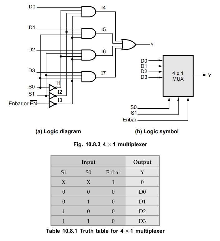
10.8.1 : 4 × 1 Multiplexer.
•
The Fig. 10.8.3 shows 4 × 1 multiplexer. Each of the four lines, DO to D3, is
applied to one input of an AND gate. Selection lines are decoded to select a
particular AND gate.
Listing
10.8.2 : HDL code of a 4 × 1 multiplexer - VHDL.
VHDL
4 × 1 Multiplexer Description,
library
ieee;
use
ieee.std_lo9ic_1164.all;
entity
mux4×1 is
port
( D : in std_logic_vector (3 downto 0);
S,
Enbar : in std_logic;
Y
: out std_logic);
end
mux4×l;
architecture
MUX of mux4×1is
signal
II, 12, 13, 14, 15, 16,17 : std_logic;
begin
-
Assume 10 nanoseconds propagation delay
-
for all and, or, and not.
11
< = not SO after 10 ns;
12
< = not SI after 10 ns;
13
< = not Enbar after 10 ns;
14
< = DO and II and 12 and 13 after 10 ns;
15
< = DI and SO and 12 and 13 after 10 ns;
16
< = D2 and SI and II and 13 after 10 ns;
17
< = D3 and SO and SI and 13 after 10 ns;
Y
< = 14 or 15 or 16 or 17 after 10 ns;
end
MUX;
7. VHDL Program Examples
Listing
10.8.3 VHDL code for half-adder.
entity
half_adder is
port
(
A:
in bit;
B:
in bit;
Sum:
out bit;
Cout:
out bit);
end
half_adder;
architecture
adder of half_adder is
begin
Sum
<= A xor B; -- signal assignment
statement.
Cout
<= A and B; -- signal assignment statement.
end
adder;
Listing
10.8.4 VHDL code of a 2 × 1 multiplexer. VHDL 2 × 1 Multiplexer Description.
library
ieee;
use
ieee.std_logic_1164.all;
entity
mux2×1 is
port
( DO, D1, S, Enbar: in std_logic;
Y:
out std_logic);
end
mux2×1;
architecture
MUX of mux2×1 is
signal
II, 12, 13, 14 : stdlogic;
begin
-
Assume 10 nanoseconds propagation delay
-
for all and, or, and not.
11
< = not S after 10 ns;
12
< = not Enbar after 10 ns;
13
< = DO and II and 12 after 10 ns;
14
< = DI and S and 12 after 10 ns;
Y
< = 13 or 14 after 10 ns;
end
MUX;
Listing
10.8.5 : VHDL code of a 2 × 2 magnitude comparator,
library
ieee;
use
ieee.std_logic_1164.all;
entity
COMP_2 is
port
( A, B : in std_logic_vector(l downto 0);
AgtB,
AltB, AeqB : out std_logic;
end
COMP 2;
architecture
COMP of COMP_2 is
begin
AgtB
< = (A(0) and not B(l) and not B(0)) or (A( 1) and not B(l))
or
A(l) and A(0) and not B(0));
AltB
<= (not A(l) and not A(0) and B(0)) or (not A(0) and B(l) and B(0))
or
(not A(l) and B(l));
AeqB
<= (A(0) xnor B(0)) and (A(l) xnor B(l));
end
COMP;
Listing
10.8.6 : VHDL code for a D-latch-VHDL
library
ieee;
use
ieee.std_logic_1164.all;
entity
D_Latch is
port
( D, EN : in std_logic;
Q,
Qbar : buffer std_logic);
-
Q and Qbar are declared as buffer because they act as
-
both input and output, they appear on the right and left
-
hand side of signal assignment statements, inout or
-
linkage could have been used instead of buffer.
end
D_Latch;
architecture
Latch of D_Latch is
constant
Delay_Nand : Time := 10 ns;
begin
Q
< = Qbar nand (D nand EN) after 2*Delay_Nand;
Qbar
< = Q nand ((D nand D) nand EN) after 3*Delay_Nand;
end
Latch;
Listing
10.8.7 : Write the HDL description of the circuit specified
by the following Boolean functions : x = A + BC + B'D, y = B'C + B C' D'
Use
continuous assignment statements.
library
ieee;
entity
ckt is
port
(A, B, C, D : in std_logic;
(x,
y : out std_logic);
end
ckt;
architecture
COMB of ckt is
begin
x
< = A or (B and C) or (not B and D);
y
< = (not B and C) or (B and (not C) and (not D));
end
COMB;
Review Questions
1. Explain the structural description with the help of example.
2. Explain different concurrent signal assignment statements
with examples
3. Differentiate concurrent and sequential signal assignment
statements.
4. Explain the constant declaration and assignment statement.
5. Explain the vector data type and its declaration.
6. Write an HDL code that implements an 8:1 multiplexer.
7. Write VHDL coding for 4
× 1 Multiplexer.
Digital Logic Circuits: Unit V: VHDL : Tag: : VHDL - Structure of Data Flow Description
Related Topics
Related Subjects

Digital Logic Circuits
EE3302 3rd Semester EEE Dept | 2021 Regulation | 3rd Semester EEE Dept 2021 Regulation