Digital Logic Circuits: Unit I: (b) Digital Logic Families
Transistor Transistor Logic (TTL)
Circuit diagram, Characteristics, Truth Table, Advantages and Disadvantages
Transistor Transistor Logic, TTL, is named for its dependence on transistors alone to perform basic logic operations. The first version, which is now known as standard TTL, was developed in 1965 and is rarely used in today's systems.
Transistor Transistor Logic (TTL)
•
Transistor Transistor Logic, TTL, is named for its dependence on transistors
alone to perform basic logic operations. The first version, which is now known
as standard TTL, was developed in 1965 and is rarely used in today's systems.
Through the years, the basic design has been modified to improve its
performance in several respects and as a consequence, a number of subfamilies
have evolved. In this section we are going to study the basic transistor
configurations in TTL and its subfamily circuits along with their
characteristics.
1. TTL Inverter
•
We have seen that when the input voltage is low, the output voltage is HIGH and
vice versa. Therefore, we can make a logic inverter from an npn transistor in
the common emitter configuration as shown in the Fig. 2.5.1.
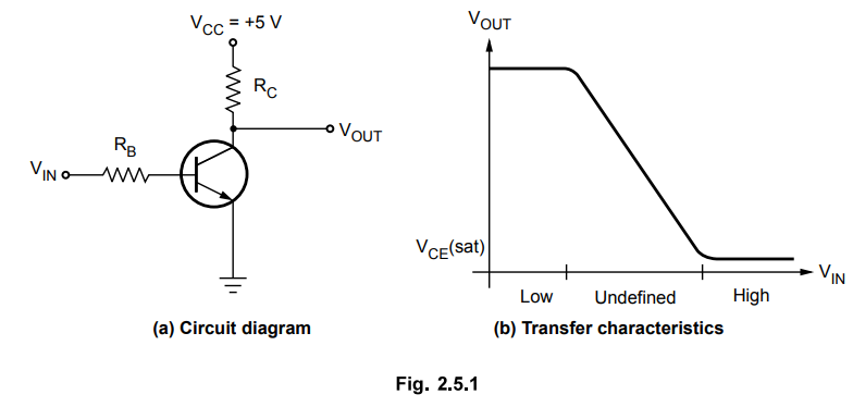
•
The Fig. 2.5.2 (a) and 2.5.2 (b) shows the operation of transistor inverter for
both the inputs (HIGH and LOW) using switching analogy.

2. 2-Input TTL NAND Gates
• The Fig. 2.5.3 (a) shows the circuit diagram of 2-input NAND gate.

Its input structure consists of multiple-emitter transistor and output structure consists of totem-pole output. Here, Q1 is an NPN transistor having two emitters, one for each input to the gate. Although this circuit looks complex, we can simplify its analysis by using the diode equivalent of the multiple-emitter transistor Qp as shown in Fig. 2.5.3 (b). Diodes D2 and D3 represent the two E-B junctions of Qi and D4 is the collector-base (C-B) junction.
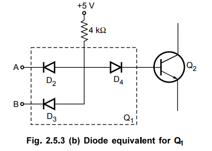
•
The input voltages A and B are either LOW (ideally grounded) or HIGH (ideally +
5 volts). If either A or B or both are low, the corresponding diode conducts
and the base of Q1 is pulled down to approximately 0.7 V. This
reduces the base voltage of Q2 to almost zero. Therefore, Q2
cuts off. With Q2 open , Q4 goes into cut-off and the Q3
base is pulled HIGH. Since Q3 acts as an emitter follower, the Y
output is pulled up to a HIGH voltage. On the other hand, when A and B both are
HIGH, the emitter diode of Q1 are reversed biased making them off.
This causes the collector diode D4 to go into forward conduction.
This forces Q2 base to go HIGH. In turn, Q4 goes into
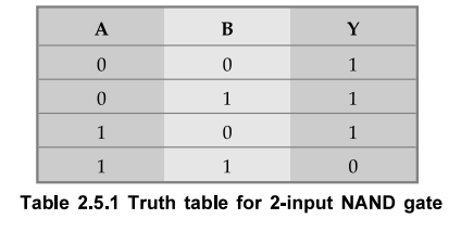
saturation, producing a low output. Table 2.5.1 summarizes all input and output
conditions.
•
Without diode D1 in the circuit, Q3 will conduct slightly
when the output is low. To prevent this, the diode is inserted; its voltage
drop keeps the base-emitter diode of Q3 reverse-biased. In this way,
only Q4 conducts when the output is low.
3. 3-Input TTL NAND Gate
• The Fig. 2.5.4 shows the three input TTL NAND gate. It is same as that of two input TTL NAND gate except that its Qi(NPN) transistor has three emitters instead of two. Rest of the circuit is same. For three input NAND gate if all the inputs are logic 1 then and then only output is logic 0; otherwise output is logic 1. The operation is similar to the 2-input NAND gate. The Table 2.5.2 shows the truth table for 3-input NAND gate.

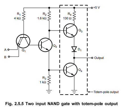
4. Totem-Pole Output
•
Fig. 2.5.5 shows an highlighted output configuration. Transistor Q3
and Q4 form a totem-pole. Such a configuration is known as active
pull-up or totem pole output. The active pull-up formed by Q3 and Q4
has specific advantage. Totem-pole transistors are used because they produce a
LOW output impedance. Either Q3 acts as an emitter follower (HIGH
output) or Q4 is saturated (LOW output). When Q3 is conducting, the
output impedance is approximately 70 Ω; when Q4 is saturated, the
output impedance is only 12 Q . Either way, the output impedance is low. This
means that the output voltage can change quickly from one state to the other
because any stray output capacitance is rapidly charged or discharged through
the low output impedance. Thus the propagation delay is low in totem-pole TTL
logic.
5. Open-Collector Output
•
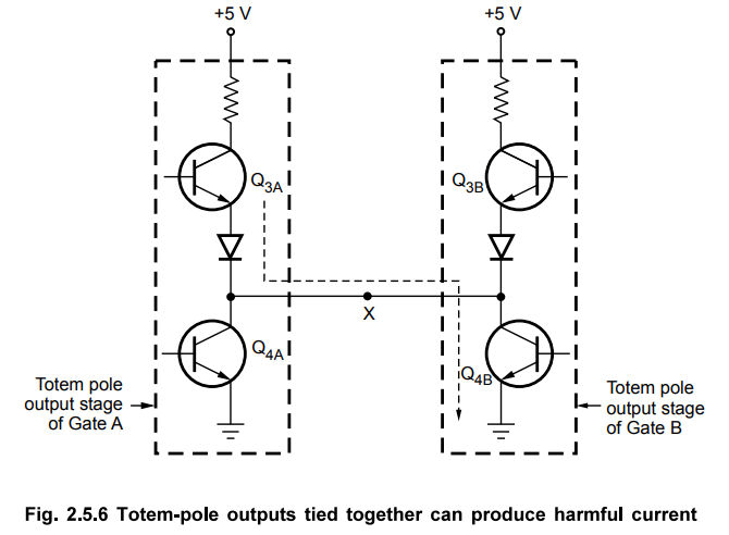
One problem with totem pole output is that two outputs cannot be tied together.
See the Fig. 2.5.6, where the totem pole outputs of two separate gates are
connected together at point X. Suppose that the output of gate A is high (Q3A
ON and Q4A OFF ) and the output of gate B is low (Q3B OFF
and Q4B ON ). In this situation transistor Q4B acts as a load for
Q3A. Since Q4B is a low resistance load, it draws high current around 55 mA.
This current might not damage Q3A or Q4B immediately, but
over a period of time can cause overheating and deterioration in performance
and eventual device failure.
•
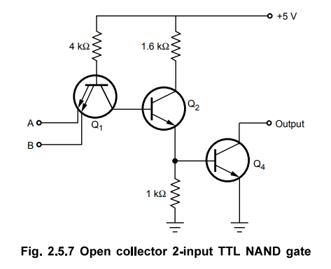
Some TTL devices provide another type of output called open collector output.
The outputs of two different gates with open collector output can be tied
together. This is known as wired logic. Fig. 2.5.7 shows a 2-input NAND gate
with an open-collector output eliminates the pull-up transistor Q3,
D1 and R4. The output is taken from the open collector
terminal of transistor Q4.
•
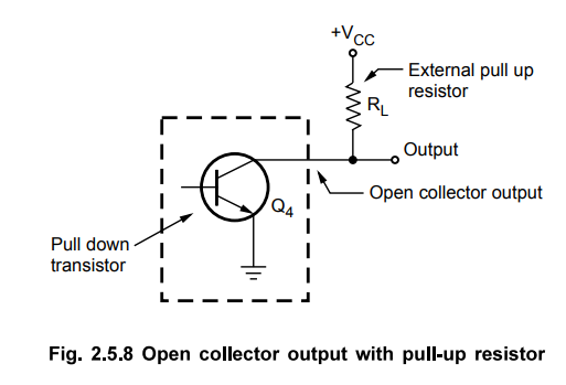
Because the collector of Q4 is open, a gate like this will not work
properly until you connect an external pull-up resistor, as shown in Fig.
2.5.8. When Q4 is ON, output is low and when Q4 is OFF
output is tied to VCC through an external pull up resistor.
•
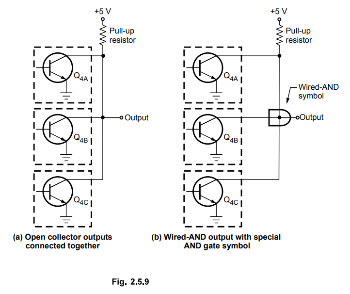
As mentioned earlier, the open collector outputs of two or more gates can be
connected together, as shown in the Fig. 2.5.9 (a). The connection is called a
wired-AND and represented schematically by the special AND gate symbol as shown
in Fig. 2.5.9 (b).
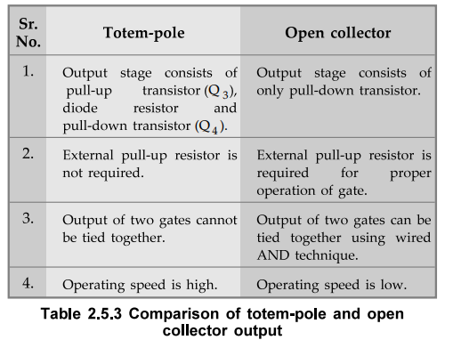
6. Comparison between Totem-Pole and Open-Collector Outputs
•
Table 2.5.3 summarizes the difference between totem-pole and open collector
outputs.
7. Tri-State TTL Inverter
•
The tristate configuration is a third type of TTL output configuration. It
utilizes the high-speed operation of the totem-pole arrangement while
permitting outputs to be wired-ANDed (connected together). It is called
tristate TTL because it allows three possible output stages : HIGH, LOW and
high-impedance. We know that transistor Q3 is ON when output is HIGH
and Q4 is ON when output is LOW. In the high impedance state both
transistors, transistors Q3 and Q4 in the totem-pole arrangement
are turned OFF. As a result, the output is open or floating, it is neither LOW
nor HIGH.
•
Fig. 2.5.10 shows the simplified circuit for tristate inverter. It has two
inputs A and E.
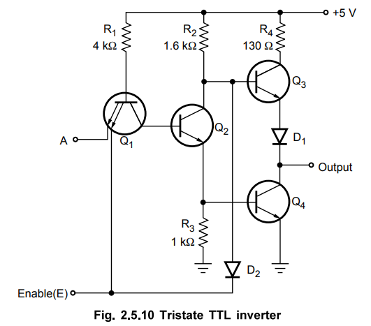
• A is the normal logic input whereas E is an
ENABLE input. When ENABLE input is HIGH, the circuit works as a normal
inverter. Because when E is HIGH, the state of the transistor Q4 (either ON or
OFF) depends on the logic input A, and the additional component diode is open
circuited as its cathode is at logic HIGH. When ENABLE input is LOW, regardless
of the state of logic input A, the base-emitter junction of Qj is forward
biased and as a result it turns ON. This shunts the current through Rx away
from Q2 making it OFF. As Q2 is OFF, there is no sufficient drive for Q4 to
conduct and hence Q4 turns off. The LOW at ENABLE input also forward-biases
diode D2, which shunt the current away from the base of Q3, making it OFF. In
this way, when ENABLE input is LOW, both transistors are OFF and output is at
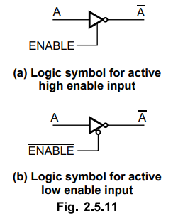
high impedance state. Fig. 2.5.11 shows the logic symbols for tristate
inverter. In above case circuit operation is enabled when ENABLE input is HIGH.
Therefore, ENABLE input is active high. The logic symbol for active high enable
input is shown in Fig. 2.5.11 (a). In some circuits ENABLE input can be active
LOW, i.e. circuit operates when ENABLE input is LOW. The logic symbol for
active low ENABLE input is shown in the Fig. 2.5.11 (b).
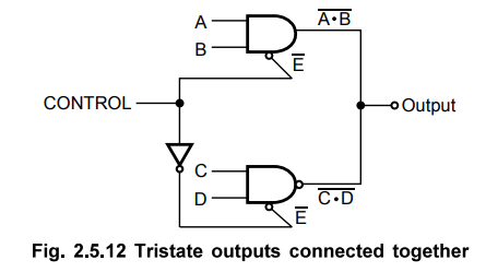
•
As mentioned earlier, tristate outputs can be connected together. This is
illustrated in Fig. 2.5.12. When CONTROL input is LOW, upper NAND gate is
enabled and its output  is available on the output terminal. The
output of lower NAND gate is in the tristate. When CONTROL input is high, the
output of upper gate is in the tristate while output of lower NAND gate
is available on the output terminal. The
output of lower NAND gate is in the tristate. When CONTROL input is high, the
output of upper gate is in the tristate while output of lower NAND gate  is available on the output terminal. The same concept is used when two or more
device shares a common bus.
is available on the output terminal. The same concept is used when two or more
device shares a common bus.
8. Characteristics of TTL Family
•
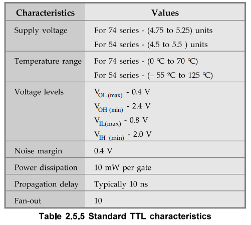
In 1964 Texas Instruments Corporation introduced the standard TTL ICs, 54/74
series. There are several series/ subfamilies in the TTL family of logic
devices. Let us see the characteristics of standard TTL family.
Supply
voltage and temperature range
•
Both the 74 series and 54 series operate on supply voltage of 5 V. The 74
series works reliably over the range 4.75 V to 5.25 V, while the 54 series can
tolerate a supply variation of 4.5 to 5.5 V. The 74 series devices are guaranteed
to work reliably over a temperature range of 0 to 70 °C where as 54 series
devices can handle temperature variations from - 55 to + 125 °C. From the above
values we can say that 54 series devices have greater tolerance of voltage and
temperature variations. Hence, these devices are used where it is necessary to
maintain reliable operation over an extreme range of conditions. For example,
in military and space application. The only disadvantage of these devices is
that they are expensive.
Voltage
levels and noise margin
•
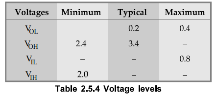
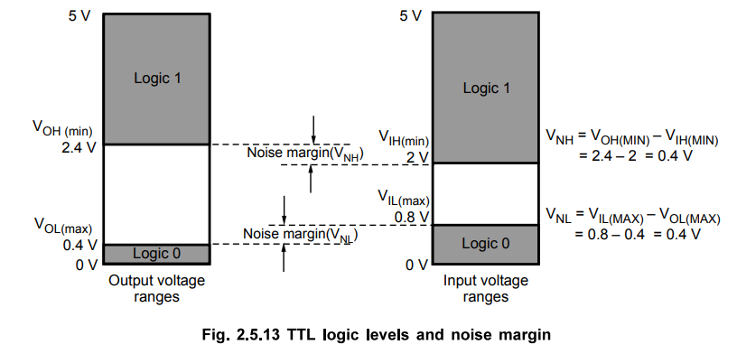
Table 2.5.4 shows the input and output logic voltage levels for the standard 74
series. The minimum and maximum values shown in the Table 2.5.4 are for worst
case conditions of power supply, temperature and loading conditions.
•
Looking
at the Table 2.5.4 we can say that, in the worst case, there is difference of 0.4
V between the driver output voltages and the required load input voltages. For
instance, the worst-case low values are
VOL(max)
= 0.4 V driver output
VIL(max)
= 0.8 V load input
Similarly,
the worst-case high values are
VOH
(min) = 2.4 V driver output
VIH (min) = 2 V load input
• In either case, the difference is 0.4 V. This difference is called noise margin. For TTL, Low state noise margin, VNL and high state noise margin, VNH both are equal and 0.4 V. This is illustrated in Fig. 2.5.13. It provides built-in protection against noise. It ensures reliable operation of the device for induced noise voltages less than 0.4 V.
Power
dissipation and propagation delay
•
A standard TTL gate has an average power dissipation of about 10 mW. It may
vary from this value because of signal levels, tolerances etc. We know that,
the propagation delay time is the time it takes for the output of a gate to
change after the inputs have changed. The propagation delay time of a TTL gate
is approximately 10 nanoseconds.
Fan-out
•
A standard TTL output can typically drive 10 standard TTL inputs. Therefore,
standard TTL has fan-out 10.
•
Table
2.5.5 summarizes the characteristics of standard TTL
9. TTL NOR Gate
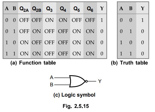
•
The
Fig. 2.5.14 shows the circuit diagram for an LS-TTL two-input NOR gate
(74LS02). The circuit is basically divided into three functional parts.
•
Input
circuits.
•
Phase
splitter.
•
Output
stage.
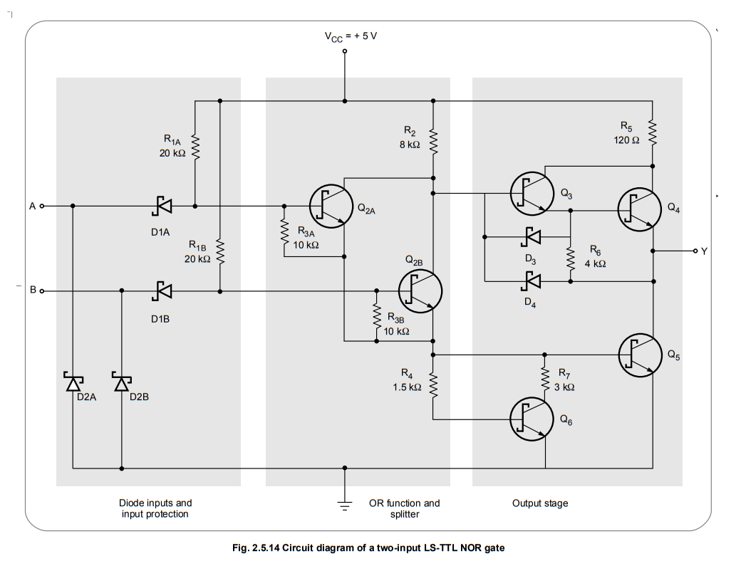
•
It is almost identical to those of an LS-TTL NAND gate. The difference is that an
LS-TTL NAND gate uses diode to perform the AND function, while an LS-TTL NOR
gate uses parallel transistors in the phase splitter to perform the OR
function.
•
If either input A or B is HIGH, the corresponding phase splitter transistor Q2A
or Q2B s turned on, which turns off Q3 and Q4
while toning on Q5 and Q6 and the output is LOW. If both
the inputs are LOW, then both phase-splitter transistors are OFF and the output
is forced HIGH. This functional operation is summarized in Fig. 2.5.15 (a). The
Fig. 2.5.15 (b) and (c) shows the truth table and logic symbol.
10. Advantages and Disadvantages of TTL Family
Advantages
of TTL
1.
High speed operation. Fastest among the saturated logic families. The
propagation delay time is about 10 ns.
2.
Moderate power dissipation.
3.
Available in commercial and military versions.
4.
Available for wide range of functions.
5.
Low cost.
6.
Moderate packaging density.
Disadvantages
of TTL
1.
Higher power dissipation than CMOS.
2.
Lower noise immunity than CMOS.
3.
Less fan-out than CMOS.
Review Questions
1. Explain the concept, operation and characteristics of TTL
family.
2. Write a short note on TTL family.
AU : Dec.-07, Marks 8
3. Draw the TTL inverter circuit.
4. Explain the working of 2 input TTL totem-pole NAND gate
circuit.
5. Explain the working of a 3-input TTL totem-pole NAND gate.
6. Explain the totem-pole output stage in TTL with circuit
diagram.
7. Draw the circuit diagram of TTL open collector two input NAND
gate.
8. Write a purpose of pull-up resistor in TTL logic family.
9. What is the difference between totem-pole output and
open-collector output in TTL logic family ?
AU : May-15, Marks 6
10 .Draw the circuit diagram and explain the working of TTL
inverter with tristate output.
AU : May-09, Marks 8
11. What is meant by tristate capability ?
12. Discuss about the TTL parameters.
AU : Dec.-04, Marks 10
13.State the important characteristics of TTL family.
AU : Dec.-l0, Marks 2
14. Name and explain the characteristics of TTL family.
15. Distinguish between 7400 series and 5400 series.
AU : May-04, Marks 2
16. State advantages and disadvantages of TTL family.
17. List the advantages of TTL logic family.
18. Draw and explain the NOR gate using TTL logic.
AU : Dec.-ll, Marks 8
19. Design a TTL logic circuit for a 3-input NAND gate.
20. With circuit schematic explain the operation of a two input
TTL NAND gate.
21. Explain the structure and working principles of TTL based
Totem-pole output configuration.
AU : Dec.-18, Marks 13
Digital Logic Circuits: Unit I: (b) Digital Logic Families : Tag: : Circuit diagram, Characteristics, Truth Table, Advantages and Disadvantages - Transistor Transistor Logic (TTL)
Related Topics
Related Subjects

Digital Logic Circuits
EE3302 3rd Semester EEE Dept | 2021 Regulation | 3rd Semester EEE Dept 2021 Regulation