Digital Logic Circuits: Unit I: (b) Digital Logic Families
Two Marks Questions with Answers
Digital Logic Families | Digital Logic Circuits
Digital Logic Circuits: Unit I: (b) Digital Logic Families : Two Marks Questions with Answers
Two Marks Questions with Answers
Q.1
Classify the basic families that belong to the bipolar families and to the MOS
families.
AU
: May-06
Ans.
:
The Fig. 2.10.1 gives the classification of families that belong to the bipolar
families and to the MOS families.

Q.2
Define noise margin.
Ans.
:
•
The voltage difference between the lowest possible HIGH output, VOH (min) and
the minimum input voltage, VIH(min) required for a HIGH input is called
high-state noise margin.
•
The voltage difference between the largest possible low output, VOL (max) and
the maximum voltage, VIL(max) required for a LOW input is called low-state
noise margin.
•
The noise margin allows the digital circuit to function properly if noise
voltages are within the noise margin.
Q.3
What is fan-out of a gate ?
AU
: Dec.-05, 08, 15, May-11, 16
Ans.
:
It is the maximum number of inputs of the same family that the gate can drive
maintaining its output levels within the specified limits.
For
example : If an inverter's output can drive maximum 10 inputs of any logic
gates from same family, the fan-out of the inverter is 10.
Q.4
What is fan-in of a gate ?
Ans.
:
Fan-in of a gate is said to be the number of inputs in a digital logic gate.
For
example : 2 input NOR has fan-in of 2.
Q.5
Define power dissipation and propagation delay.
AU
: May-05, 15
Ans.
:
Power dissipation is the product of ICC and VCC, where ICC
is the average supply current and VCC is the supply voltage.
It is given as :
Power
dissipation PD = ICC × VCC.
The
propagation delay of a gate is basically the time interval between the
application of an input pulse and the occurrence of the resulting output pulse.
Q.6
Why does the propagation delay occur in logic circuits ?
Ans.
:
Propagation delay occur in logic families due to following reasons :
1.
The intrinsic delay of the gate itself, also known as internal delay (tpo).
2.
The delay introduced by fan-outs of a logic gate. It is denoted as tpL.
Hence,
for a fan-out of N of a gate, the propagation delay (tp) is
approximately,
tp = tPo + tpL
3.
While logic gate levels are cascaded then resulting propagation delay will be
addition of propagation delays of each level.
Q.7
What do you mean by logic levels ? Explain positive logic and negative logic
systems ?
Ans.
:
The two voltage levels used to represent two logic states in digital logic are
called logic levels.
The
system in which the higher of the two voltage levels represent a 1 and the
lower voltage represents a 0 is called a positive logic system.
Positive
Logic HIGH = 1 (i.e. +5 V)
LOW
= 0 (i.e. 0 V)
The
system in which the lower of the two voltage levels represent a 1 and the
higher of the voltage represents a 0 is called a negative logic system.
Negative
Logic
HIGH
= 0 (i.e. + 5 V)
LOW
= 1 (i.e. 0 V)
Q.8
What are the advantages of digital integrated circuits ?
Ans.
:
Advantages of digital integrated circuits are :
1.
The traditional method of designing combinational circuit is effective for
small circuit. But time consuming and less reliable for complex circuits
digital ICs take care of this problem.
2.
Digital ICs reduce system cost.
3.
They are smaller in size.
4.
Less power is required for the system.
5.
Lesser number of external wire connections which improves reliability of the
system.
6.
Depending upon circuit complexity, any of the 5 levels of integration can be
chosen.
Q.9
Define speed power product.
Ans.
:
Speed power product is the product of propagation delay and average power
dissipation. It is a means for measuring and comparing the overall performance
of an IC family. It is given as :
Speed
power product (J) = Propogation delay (seconds) × Power dissipation (J / sec)
Q.10
Mention the important characteristics of digital IC’s?
Ans.
:
The important characteristics of digital IC's are :
1.
Fan out 2. Power dissipation 3. Propagation delay 4. Noise margin
5.
Fan in 6. Operating temperature 7.
Power supply requirements.
Q.11
What is operating temperature ?
Ans.
:
All the gates or semiconductor devices are temperature sensitive in nature. The
temperature in which the performance of the IC is effective is called operating
temperature. Operating temperature of the IC vary from 0 °C to 70 °C.
Q.12
When does the noise margin allow digital circuits to function properly ?
Ans.
:
When noise voltages are within the limits of (High state noise margin and low
state noise margin for a particular logic family; the digital circuits are
allowed to function properly.
Q.13
Define rise time and fall time.
Ans.
:
•
Rise time is the time required to switch from 10
•
Fall time is the time required to switch from 90 % of the voltage level to 10 %
of voltage level.
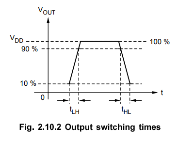
Q.14
Explain output switching times using waveform.
Ans.
:
The finite time taken by a circuit to change output levels is called output
switching time. There are 2 terms of great significance in output switching
times. They are : tLH (rise time) and tHL (fall time). The minimum amount of
time needed for a gate to switch from 0 to 1 and back is given by
tmin
tLH + tHL
Q.15
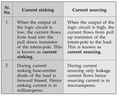
Differentiate: Source and sink current.
AU
: May-07
Ans.
:
Q.16
Draw circuit diagram of 2-input RTL NOR gate. (Refer section 2.3.1)
Q.17
List any four important specifications of RTL family. (Refer section 2.3.3)
Q.18
State the advantages of DTL over RTL. (Refer section 2.4)
Q.19
Draw circuit diagram of 2-input DTL NAND gate. (Refer section 2.4.1)
Q.20
List any four important specifications of DTL family. (Refer section 2.4.3)
Q.21
What are the types of TTL logic?
Ans.
1.
Open collector output
2.
Totem-pole output
3.
Tri-state output.
Q.22
List the different versions of TTL.
Ans.
:
1.
TTL (Std.TTL)
2.
LTTL (Low Power TTL)
3.
HTTL (High Speed TTL)
4.
STTL (Schottky TTL)
5.
LSTTL (Low Power Schottky TTL)
Q.23
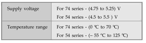
Distinguish between 7400 series and 5400 series.
AU
: May-04
Ans.
:
Q.24 What is meant by tristate capability ?
Ans.
:
Tristate capability is the capability of output level to take three stages (output
levels) as HIGH, LOW and High-impedance. For example, tristate TTL.
Q.25
Explain open collector output.
Ans.
:
When the collector terminal of a transistor is kept open without any pull up
transistor the arrangement is called open collector output. The output is taken
directly from the open collector terminal of a transistor at the output. But, a
gate with open collector will not work properly until an external resistor is
connected.
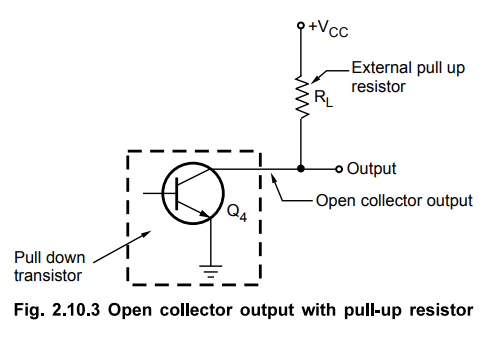
When
Q4 is ON, output is low and when Q4 is OFF, output is
tied to VCC through an external pull up resistor.
Q.
26 Compare the totem-pole and open-collector outputs.
(Refer
Table 2.5.3)
Q.
27 Describe the characteristics of TTL family.
(Refer
Table 2.5.8)
Q.
28 How Schottky transistors are formed and state its use ?
Ans.
: A
Schottky diode is formed by the combination of metal and semiconductor. The
presence of schottky diode between the base and the collector prevents the
transistor from going into saturation. The resulting transistor is called
Schottky transistor.
The
use of Schottky transistor in TTL decreases the propagation delay without a
sacrifice of power dissipation.
Q.29
Why totem pole outputs cannot be connected together ?
Ans.
:
Totem pole outputs cannot be connected together because such a connection might
produce excessive current and may result in damage to the devices.
Q.30
What happens to output when a tristate circuit is selected for high impedance ?
Ans.
:
Output is disconnected from rest of the circuits by internal circuitry.
Q.31
State advantages and disadvantages of totem-pole output.
Ans.
:
Advantages of totem-pole output are :
1.
External pull up resistor is not required.
2.
Operating speed is high.
Disadvantages
of totem-pole output :
1.
Output of two gates cannot be tied together.
Q.32
Explain the wired-AND connection.
Ans.
:
When the open collector outputs of two or more gates can be connected together,
the connection is called a wired AND. In wired-AND connection, the output is
high only when all switches are open i.e. when output of each stage is high.
Hence,
the output is equivalent to the logical AND operation of the logic function
performed by the gates.
Q.33
Give any two applications of open collector logic.
AU
: May-07
Ans.
: 1. It is used when we require to
connect outputs of two or more gates.
2.
It is used when sourcing current requirements is larger than the standard
totem-pole output.
Q.34
State advantages and disadvantages of TTL
(Refer
section 2.5.10)
Q.35
List the advantages of ECL as compared to TTL logic family.
Ans.
:
Advantages of ECL over TTL logic family are as follows :
1.
In ECL, as transistors are not allowed to go into complete saturation, storage
delays are eliminated.
2.
ECL has a small voltage swing, less than a volt. Hence propagation delays are
very short as short as 1 ns.
3.
Switching transients are less because power supply current is more stable than
in 1 I L and CMOS circuits.
Q.36
What is the major difference between ECL and TTL ?
Ans.
:
The major difference between ECL and TTL are :

Q.
37 Which is faster TTL or ECL? Which requires more power to operate?
Ans.
:
ECL
is faster and requires more power to operate.
Q.38
What is the effect of increasing the supply voltage on the propagation delay of
the CMOS gates ?
AU
: May-09
Ans.
:
Increasing the supply voltage reduce the propagation delay of the CMOS gates.
Q.39
Which IC family offers (a) Low propagation delay and (b) Low power dissipation
?
Ans.
:
a) ECL b) CMOS
Q.40
Give the comparison between TTL, CMOS and ECL.
(Refer section 2.8)
Q.41
Why should we take care while using CMOS devices ?
Ans.
:
We should take care while using CMOS devices because these devices are highly
prone to damage by electrostatic discharge.
Q.42
What are the advantages of CMOS ?
(Refer
section 2.6.7)
Q.43
List the factors used for measuring the performance of digital logic families.
(Refer
section 2.2)
Q.44
Draw the DTL based NAND gate.
(Refer
section 2.4)
Digital Logic Circuits: Unit I: (b) Digital Logic Families : Tag: : Digital Logic Families | Digital Logic Circuits - Two Marks Questions with Answers
Related Topics
Related Subjects

Digital Logic Circuits
EE3302 3rd Semester EEE Dept | 2021 Regulation | 3rd Semester EEE Dept 2021 Regulation