Digital Logic Circuits: Unit II: Combinational Circuits
Two Marks Questions with Answers
Combinational Circuits | Digital Logic Circuits
Digital Logic Circuits: Unit II: Combinational Circuits : Two Marks Questions with Answers
Two Marks Questions with Answers
Q.1
What do you mean by literal ?
Ans.
:
Definition : In Boolean Function, the total number of variables in
complemented or uncomplemented form are called literals.
For
example : 
Q.2
State two absorption properties of Boolean algebra.
Ans.
: 1.
A + AB = A. 2. A (A + B) = A
Q.3
State the associative law of Boolean algebra.
Ans.
:
Associative laws are as follows :
1.
Law 1 (The associative law of addition) :
In
the Oring of serveral variables, the result is the same regardless of the
grouping of the variables. For three variables, A ORed with B OR C is the same
as A OR B ORed with C.
i.e.
A + (B + C) = (A + B) + C
2.
Law 2 (The associative law of multiplication) :
It
makes no difference in what order the variables are grouped when ANDing several
variables. For three variables, A AND B ANDed with C is the same as A ANDed
with B and C.
i.e.
(AB) C = A(BC)
Q.4
Explain the De Morgan's theorem in Boolean Algebra. (Refer section 3.1.3.3)
AU
: May-11, Dec.-12, June-14
Q.5
Explain the principle of duality with the help of example.
Ans.
:
The duality theorem says that, starting with a Boolean relation, you can derive
another Boolean relation by -
1.
Changing each OR sign to an AND sign
2.
Changing each AND sign to an OR sign and
3.
Complementing any 0 to 1 appearing in the expression.
For
example : A + 0 = A. Using duality theorem, we can say that, A • 1 = A.
Q.6
State and prove the consensus theorem in Boolean algebra.
Ans.
:
Definition : In simplification of Boolean expression, the redundant term
in an expression can be eliminated to form the equivalent expression. The
theorem used for this simplification is called consensus theorem. For example,
in expression of the  the term BC is redundant and can be
eliminated using consensus theorem.
the term BC is redundant and can be
eliminated using consensus theorem.

Q.7
Name the two basic types of Boolean expressions.
Ans.
:
There are two basic types of Boolean expressions are :
•
Sum of product Form (SOP) and
•
Product of Sum Form (POS)
Q.8
Name the two canonical forms for Boolean algebra.
Ans.
:
Standard SOP and standard POS forms.
Q.9
Express F = BC' + AC in a canonical SOP form.
AU
: Dec.-03
Ans.
:
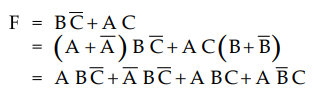
Q.
10 How many inputs are required for 
Ans.
:
6-inputs
Q.
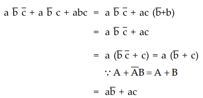
11 Simplify the following Boolean expression to a minimum number of literals:

Q.
12 Simplify the Boolean expression 
Ans.
:
Q.
13 Simplify : x + xy
Ans.
:

Q.
14 Show that
a)
a + a’ b = a + b
b)
x’y’z + x’ yz + xy’ = x’z + xy’
Ans.
:
a)
Refer example 3.1.1.

Q.15
What is variable mapping ?
Ans.
:
Representing the minterms of the sum of product expression in the Kamaugh-map
of appropriate variables is known as variable mapping.
Q.16
What code is used to label the row headings and column heading of K-map and why
?
Ans.
:
•
Gray code is used to label the rows and columns of K-map.
•
In case of Gray code, only one variable changes between two consecutive
number.This is useful in grouping pair, quad, or octets in k-maps and thus
eliminating variables in the final expression. Hence, Gray code is used to
label the rows and columns of K-map.
Q.17
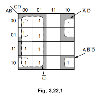
Show the Karnaugh map with the encircled groups for the Boolean function,
AU
: May-07
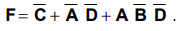
Ans.
:
Q.18
What are don't care conditions and incompletely specified functions ?
Ans.
:
Sometimes, while designing a digital circuit, certain conditions of input are
of no use. Consider an example of BCD input for a seven segment display. In
this case, inputs from 0 through 9 are valid inputs. Thus, rest of the inputs
from 10 through 15 do not signify anything at the output side. The outputs for
which inputs are not specified are called don’t care outputs. The Boolean
function in which don’t care outputs exists is called incomplete Boolean
function or incompletely specified functions.
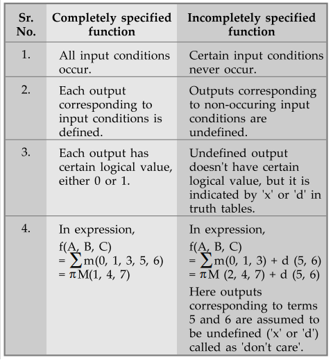
Q.19
Distinguish between completely specified function and incompletely specified
function.
Ans.
:
Q.
20 What are prime implicants?
Ans
. :
All the implicants of a function determined using a Karnaugh map are called
prime implicants.
Q.21
State two significant features of tabular method of minimization of Boolean
functions.
Ans.
: 1. It is an exact method to simplify
the Boolean expression.
2.
It can be used to simplify expression with 7, 8 or even 10 variables.
Q.22
Define binary logic ?
Ans.
:
Binary logic consists of binary variables and logical operations. The variables
are designated by the alphabets such as A, B, C, x, y, z, etc., with each
variable having only two distinct values: 1 and 0. There are three basic logic
operations: AND, OR, and NOT.
Q.23
What is a logic gate ?
Ans.
:
The logic gate is an electronic circuit that has one or more input binary
variables but only one output. It is called logic gate because of it ability to
operate on a number of binary inputs to perform a logical function, i.e. its
output is a logical function of inputs.
Q.
24 What are the basic digital logic gates ?
Ans.
:
The three basic logic gates are • AND gate • OR gate • NOT gate
Q.
25 Draw the logic symbol and construct the truth table of the following gates :
a)
Three input OR gate b) Three input EX-NOR gate
Ans
. :
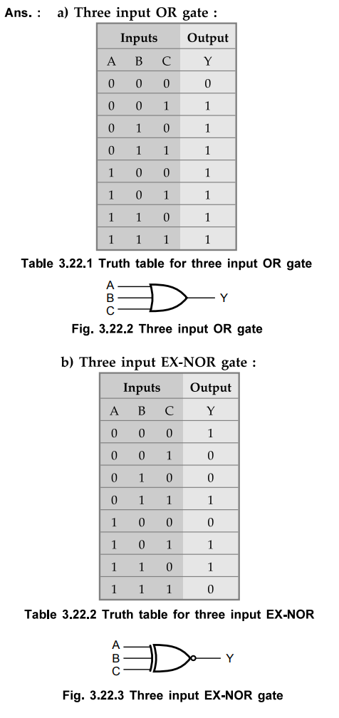
Hint
:
For even number of ones output is one
Q.26
Give the Boolean expression used for following gates
a)
AND b) NOR c) EX-OR d) OR e) NOT
Ans.
:
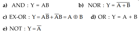
Q.27
Which gate is equal to AND-invert Gate ?
Ans.
:
NAND gate.
Q.28
Which gate is equal to OR-invert Gate ?
Ans.
:
NOR gate.
Q.29
Bubbled OR gate is equal to .
Ans.
:
NAND gate.
Q.30
Bubbled AND gate is equal to .
Ans.
:
NOR gate.
Q.31
Write the names of Universal Gates
Ans.
:
Universal gates are : NAND gate and NOR gate.
Q.32
Why are NAND and NOR gates known as Universal gates ?
Ans.
:
NAND and NOR are the gates that can be used alone to generate remaining gates
such as NOT, AND and OR. Thus, with only any of the two gates, we can implement
the logic circuit. Hence, they are called Universal gates.
Q.33
Why digital circuits are more frequently constructed with NAND or NOR gates
than with AND and OR gates ?
Ans.
:
Digital circuits are frequently constructed with NAND or NOR gates due to
following reasons,
•
If any simple combinational circuit we want to build and we are not using
universal gates then we want several AND, OR and NOT gates. This demands number
of ICs, one for each type of gate. For example, IC 7408 is for 2-input AND
gate, IC 7432 is for 2-input OR gate. Hence, there is possibility that all
gates in each IC are not used and IC utility factor will be poor.
•
By using universal gates it is possible to reduce number of ICs required to
implement combinational circuit.
Q.34
Implement EX-OR gate using only NAND gate. (Refer example 3.9.1)
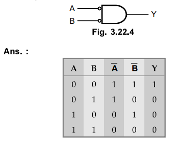
Q.35 Show that a bubbled AND gate works like a NOR gate.
Q.
36 How can a NAND gate be used as are?
Ans.
:
Q.37
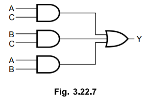
Realize the function  by using only NAND gates.
(Refer
example 3.9.3)
Q.38
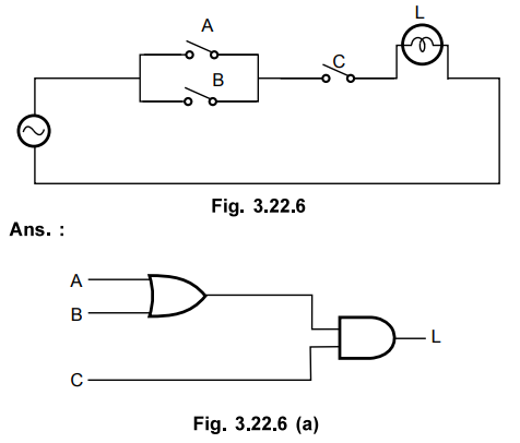
Express the following switching circuit in binary logic notation.
Q.39
Write down the truth table of XOR gate. Give an application for XOR function.
AU
: May-08
Ans.
:
For truth table : Refer section 3.9.1.
Application
for XOR function : XOR function can be used as an inverter
by connecting one input to logic 0. It can also be used as a modulo 2 adder.
Q.40
What do you mean by shared term ? Explain its significance.
Ans.
:
Sometimes, it may happen that simplified output functions may have common
terms. The common terms which are implemented only once and used by more that
one functions to generate final output are called shared terms.
Sharing
of the terms reduces product terms. Sharing of common terms reduce the total
number of gates.
Q.41
How does don't care condition in k-map help for circuit simplification ?
Ans.
:
Circuit designers are free to make the output for any don't care condition
either a 'O' or 'I' according to grouping requirements and thus eliminating
variables in the expression. This way don't care condition in k-map help for
circuit simplification.
Q.42
Define a combinational logic circuit. Give an example.
Ans.
:
When logic gates are connected together to produce a specified output for
certain specified combinations of input variables, with no storage involved,
the resulting circuit is called 'combinational logic circuit'.
A
combinational circuit consists of input variables, logic gates and output
variables. For example, consider following Boolean expression,
Y
= AB + BC + AC
The
combinational logic circuit for this would require 3 AND gates and 1 OR gate as
follows :
Q.43
Define half adder and full adder.
Ans.
:
•
Half adder : The logic circuit which performs the
arithmetic sum of two bits is called a half adder.
•
Full adder : The logic circuit which performs the
arithmetic sum of 3 bits (bit 1 : input 1, bit 2 : input 2, bit 3 : carry from
the previous addition) is called a full adder.
Q.44
Define half subtractor and full subtractor.
Ans.
:
•
Half subtractor : It is a combinational circuit that
subtracts two bits and produces their difference and borrow.
•
Full subtractor : It is a combinational circuit that
performs a subtraction between 2 bits. It also takes into account borrow of the
lower significant stage.
Q.
45 Give the circuit of a half adder-subtractor. (Refer sections 3.11.1 and
3.12.1)
Q.
46 Describe the truth table of a half subtractor and write the Boolean
expression corresponding to the difference and the borrow.
(Refer
section 3.12.1)
Q.
47 Implement half adder using gates.
(Refer
section 3.11.1)
Q.
48 What is the difference between half adder and full adder?
Ans.
:
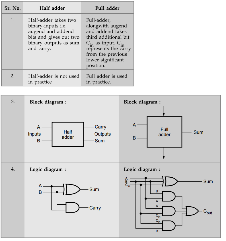
Q.49
What do you mean by carry propagation delay ?
Ans.
: Definition : In parallel adders, sum and carry
outputs of any stage cannot be produced until the input carry occurs. This time
delay in the addition process is called carry propagation delay. This delay
increases with increase in the number of bits to be added in an adder circuit.
Q.50
What do you mean by comparator ? OR Write a short note on 1-bit comparator.
Ans.
:
It is a special combinational circuit designed primarily to compare the
relative magnitudes of two binary numbers. An n-bit comparator receives two
n-bit numbers, A and B, outputs are : A > B, A = B and A < B. As per the
magnitudes of the two numbers, one of the outputs wall be high.
Q.51
What do you mean by encoder ?
Ans.
:
An encoder is a digital circuit that performs the inverse operation of a
decoder. Encoder has 2n (or fewer) input lines and n output lines. Encoder has
enable inputs to activate encoded outputs.
Q.52
Write a short note on priority encoder. OR What is a priority encoder ?
AU
: May-12
Ans.
:
A priority encoder is an encod™er circuit in which if two or more inputs are
equal to 1 at the same time, the input having the highest priority will take
precedence.
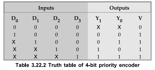
•
As per the table, when D3 is high, regardless of other inputs, the
output is 11.
•
D2 has next priority, thus, with D2 = 1 and D3
= 0, output will be 10.
•
Output for D1 is generated only if higher priority inputs are 0, and
so on.
•
If all inputs are 0, two outputs of the circuit are not used.
Q.53
What is decoder ?
Ans.
:
A decoder is a multiple - input, multiple-output logic circuit which converts
coded inputs into coded outputs, where the input and output codes are
different. In a binary decoder n-inputs produce 2n outputs. Usually,
a decoder is provided with enable inputs to activate decoded output.
Q.54
What is binary decoder ?
Ans.
:
A decoder is a combinational circuit that converts binary information from n
input lines to a maximum of 2n outputs lines.
Q.55
What will be the maximum number of outputs for a decoder with a 6 bit drd ?
Ans.
:
26 = 64.
Q.56
What is a data selector ? or what is multiplexer ? or Why is MUX called as data
detector ?
Ans.
:
•
Multiplexer is a digital switch. Particularly, it has 2n input lines and n
selection lines whose bit combinations determine which input line is selected
and routed onto available only single output line.
•
Hence, multiplexer is a selector of one out of several data sources available
at its input lines, to connect it to output line. Simply it is a 'many into
one' device and also called 'data selector'.
Q.57
Mention the differences between DMUX and MUX. (Refer section 3.18)
Q.58
Give an application each for a multiplexer and a demultiplexer.
(Refer
sections 3.17.7 and 3.18.4)
Q.59
With a aid of block diagram clearly distinguish between a decoder and encoder.
Ans.
:
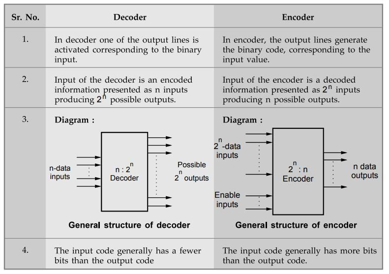
Q.60
Distinguish between a demultiplexer and decoder.
Ans.
:

Q.61
Giue one application each for Multiplxer and Decoder.
Ans.
:
Applications of Decoder are :
•
Code converters
•
Implementation of combinational circuits
•
Address decoding
•
BCD to 7-segment decoder.
Refer
section 3.17.7 for applications of multiplexer.
Q.
62 Draw a 4 × 16 decoder constructed with two 3 × 8 decoders.
(Refer
Section 3.19)
Q.
63 Mention the uses of decoders.
(Refer
section 3.19)
Q.
64 Design a half subtractor.
(Refer
section 3.12.1)
Q.
65 Construct OH gate and AND gate using NAND gates. (Refer section 3.9.2.1)
Q.
66 Draw the truth table of 2 : 1 MUX. (Refer section 3.17.1)
Q.
67 Reduce a(b+ be' + ab'.
Q.
68 Write the POS form of the SOP expression f(x,y,z) = x'yz + xyz' + xp'z.
Q.69
Design a Half Subtractor. (Refer section 3.12.1)
Q.70
What is a K-map ? (Refer section 3.3)
Q.71
Mention the dependency of output in combinational circuits.
(Refer section 3.10)
Digital Logic Circuits: Unit II: Combinational Circuits : Tag: : Combinational Circuits | Digital Logic Circuits - Two Marks Questions with Answers
Related Topics
Related Subjects

Digital Logic Circuits
EE3302 3rd Semester EEE Dept | 2021 Regulation | 3rd Semester EEE Dept 2021 Regulation