Linear Integrated Circuits: Unit I: IC Fabrication
Two Marks Questions with Answers
IC Fabrication | Linear Integrated Circuits
Linear Integrated Circuits : Unit I: IC Fabrication : Two Marks Questions with Answers
Two Marks Questions with Answers
Q.1
List the advantages of integrated circuits over discrete component circuit.
May-06,
11, 13, 15, Dec.-14, 16
Ans. : The various advantages of the integrated circuits are as follows :
i) Practically size of an IC is thousands of times smaller than the discrete circuits, which increases the equipment density.
ii) Thousands of silicon wafers consisting individually millions of components, can be produced or manufactured simultaneously, known as mass production. Due to this, the cost of IC is very very low.
iii)
As the number of components are fabricated on a single silicon wafer, which are
not similar to the conventional one, the weight of IC reduces as compared to
the discrete circuits with same number of components.
iv)
ICs operate at low voltages. The power consumption of ICs is very low.
v)
In ICs, soldered joints are absent and thus the high reliability of the system
is the main feature of ICs.
vi)
As power consumption is less, the temperature rise is also low which increases
reliability, accuracy and life of the ICs.
Q.2
What are the limitations of integrated circuits ?
Ans.
:
The disadvantages of integrated circuits are,
1.
The capacitors more than 30 pF cannot be fabricated.
2.
The resistors more than 100 k£2 cannot be fabricated.
3.
The coils or inductors cannot be fabricated.
4.
The ICs can handle limited amount of power.
5.
The ICs are delicate hence extra care must be taken while using them.
6.
The ICs function at low voltages.
7.
If any one component fails, the entire IC is to be replaced.
Q.3
Give classification of integrated circuits on the basis of application, device
used and chip complexity.
OR
What
are major categories of integrated circuits?
OR
How
ICs are classified based on the device density ?
Ans.
:
Depending upon the functional utility, the integrated circuits are classified
as linear ICs and digital ICs. From the point of view of structural
considerations, ICs can be divided as monolithic ICs, thick-thin film ICs and
hybrid ICs.
On
the basis of the active devices used, the ICs are classified as bipolar ICs and
unipolar ICs.
Depending
upon the isolation technique used, the bipolar ICs are further classified as
p-n junction isolation ICs and dielectric isolation ICs.
Depending
upon the type of FET used, the unipolar ICs are further classified as MOSFET
unipolar ICs and JFET unipolar ICs.
Q.4
Differentiate between thin film and thick film technology in 1C fabrication.
Dec.-07
Ans.
:
Generally thick-thin film ICs are used to produce only passive elements. The
thick film technology is comparatively easier and inexpensive while the thin
film technology is slightly complicated and expensively. The thin film
technology produces components with greater precision as compared to those
produced by the thick film technology.
Q.5
What are different levels of integration ?
Ans.
:
Depending upon the number of active devices per chip, there are different
levels of integration. When the active devices per chip are less than 100, then
it is referred as small scale integration (SSI). When the count of active
devices per chip is between 100 to 1000, then it is referred as medium scale
integration (MSI). In large scale integration (LSI) ICs, the number of active devices
per chip ranges between 1000 to 100,000. When the active devices per chip are
over hundreds of thousands, then it is referred as very large scale integration
(VLSI). Almost all modem chips employ VLSI technique.
A
new level of integration has been introduced which is known as ultra large
scale integration (ULSI). In ULSI technique, more than one million active
devices are integrated on a single chip.
Q.6
What do you mean by monolithic process ?
Ans.
:
The process in which all the active as well as passive elements or components
along with their interconnections are manufactured on a single silicon crystal
is known as monolithic process.
Q.7
What is meant by hybrid ICs ?
Ans.
:
The hybrid ICs are the integrated circuits used for high power application. The
hybrid ICs may combine two or more monolithic ICs or combine monolithic ICs
with thick-thin film IC in one single package.
Q.8
What is meant by planar technology ?
Ans.
:
The fabrication of different discrete devices such as diodes, transistors and
integrated circuits is carried out by the same technology. The various
processes involved in the fabrication of different devices are carried out in a
single plane. Hence this is also referred as a planar technology.
Q.
9 List basic planar processes involved in IC fabrication.
Ans.
:
1.
Crystal growth and wafer preparation.
3.
Oxidation.
5.
Reactive plasma etching.
7.
Ion implantation.
9.
Assembly techniques and packaging.
Q.
10 Why silicon is preferred as basic material for fabrication of semiconductor
devices ?
Ans.
:
1)
It is comparitively suitable for all applications as junction leakage currents
are negligible as the energy band gap is comparitively broader (1.1 eV).
2)
Silicon devices can be operated upto 200 °C temperature.
3)
Silicon dioxides are the most wanted for the planar processes.
4)
The intrinsic resistivity without any dopant is 230,000 Ω-cm hence most
suitable for high voltage rectifying devices as well as infrared sensing
devices.
5)
Silicon is cheaper as compared to germanium.
Q.11
What is meant by crystal growth ? How it is carried out ?
Ans.
:
Basically silicon is the element, found in nature in the form of silica and
silicates. It is found abundantly in the natrure in the form of silicon
dioxide. So this silicon dioxide constitutes almost 20 % of the earth's crust.
So obviously one can not start fabricating integrating circuits using silicon
dioxide with the earth's crust. The sand can be converted into pure silicaon
through number of processes. For the fabrication of ICs, the silicon must be in
crystalline form. The crystalline form of silicon is the pure silicon with no
deflects and no contaminations. For fabrication of ICs a crystalline silicon is
needed. The single crystal silicon can be obtained by using method known as
crystal growth. The primary method of the crystal growth is Czochralski (CZ)
method.
Q.12
In the Czochralski crystal growth process under what gas does crystal pulling
carried out?
Ans.
:
In general, during Czochralski crystal growth process, the gas used is argon.
Q.13
Explain briefly about in got slicing.
Ans.
:
The slices of the ingot are called wafers and typically the thickness of wafer
may very from 0.4 mm to 1 mm. This process is very important as it is necessary
to maintain the flat plane and desired surface orientations. The slicing also
determines the orientation of the surface. In general, there are two
orientations < 100 > and < 111 >. Out of these orientations, the
wafers with < 100 > orientations are cut 'on orientation' ; while wafers
with < 111 > orientations are cut 'off orientations'.
Q.14
What is meant by wafer etching ?
Ans.
:
Due to the machining operations during trimming, grinding and slicing, the
surface and edges of the wafers get contaminated and even damaged. The depth of
damage depends on the mechanical operations carried previously. It is observed
that the damaged and contaminated regions are not more than 10 pm deep. Even by
using chemical etching process, all the damaged and contaminated edges can be
removed. Practically mixture of hydrofluoric, acetic and nitric acids is used
in chemical etching. This is called acidic etching.
Q.15
What is epitaxial growth ?
Ans.
:
In epitaxy a monocrystalline film is formed on the top of a monocrystalline
surface. Thus epitaxy is crystalline growth process in which the foundation
layer i.e. substrate works as seed crystal.
Q.16
Write chemical reaction representing epitaxial growth of pure silicon.
May-11
Ans.
:
The epitaxial growth of pure silicon can be represented with the help of
following chemical reaction.
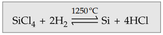
Q.17
List types of epitaxy and explain.
Ans.
:
When the epitaxial layer and the substrate on which the epitaxial layer is to
be formed, are of same materials, then the process is called homoepitaxy.
When
the epitaxial layer and the substrate on which the epitaxial layer is to be
formed are not of identical material, then the process is called heteroepitaxy.
Q.18
Write down advantages of epitaxial process.
Ans.
:
1)
Because of one or more buried layers, the designer can control the doping in
the structure.
2)
The properties of the epitaxial layer and the bulk material are different
3)
Using epitaxial structures the performances of RAMs (Random access memories)
and CMOS ICs can be improved.
Q.19
What is vapour phase epitaxy ?
Ans.
:
In chemical vapour deposition (CVD), the film is formed on the surface of the
substrate by thermal decomposition and or the reaction of various gaseous
compounds. As in CVD, the epitaxial layer is formed from the gaseous vapour
phase, hence it is called vapour phase epitaxy.
Q.20
Explain briefly molecular beam epitaxy.
Ans.
: The molecular beam epitaxy (M6E) is based on evaporation. In MBE, the film is
evaporated and deposited one layer at a time. In the process, no chemical
reactions are considered. Instead of that the evaporation of silicon and other
dopant is carried out under ultra high vacuum (UHV) pressures of the orders of
10-8 to 10-10 Torr.
Q.21
List advantages of MBE over CVD process.
Ans.
: 1)
MBE is low temperature process which is advantageous for VLSI technology.
2)
While preparing thin layers using MBE process, autodoping and autodiffusion
both are minimized.
3)
The MBE process can be used for generating complicated doping profiles as it
regulates the amount of dopant.
4)
As MBE process is based on the evaporation of silicon and the dopants, hence no
chemical reactions are involved in it.
5)
For MBE process safety precautions are not required extensively as compared to
those required in CVD process.
Q.22
What is meant by oxidation ?
Ans.
: The
process in which a thin layer of silicon dioxide (SiCh) formed on a surface of
silicon wafer using thermal growth technique is called oxidation.
Q.23
Explain importance of SiO2 layer.
Ans.
:
In the planar process it is essential to protect certain regions of surface of
the wafer so that the dopant atoms may be driven into other selective regions
during the processes such as diffusion or ion implantation. For such shielding
purpose, silicon dioxide (SiO2) is best suited.
Q.24
What are different techniques used for oxidation ?
Ans.
: i) Thermal oxidation.
ii)
Wet anodization or oxidation.
iii)
Vapour-phase technique (CVD).
iv)
Plasma anodization or oxidation.
Q.25
Define following terms : Thermal oxidation, dry oxidation, wet oxidation.
Ans.
:
The oxidation processes is called thermal oxidation because to grow the oxide
layer, the temperature maintained is high. For thin oxides with low charge
density at interface, the oxides are grown in dry oxygen. This is also called
dry oxidation. For thick layers of oxides, steam or water vapour is used at
high pressure for oxidation. This is called wet oxidation.
Q.26
How surface layer of SiO2 is formed ?
Ans.
: The surface layer of SiO2 is formed by using oxidation process. In general,
thermal oxidation technique is preferred practically to grow thin oxide layers.
Another techniques used are vapour-phase oxidation and plasma anodization.
Q.27
Name the parameters which govern the thickness of the film in the oxidation
process.
Ans.
:
The main important parameter which governs the thickness of the film in the
oxidation process is temperature. Because to grow the oxide layer high
temperature is to be maintained. The other important parameters governing oxide
film thickness are time upto which process is to be carried out and the
moisture contents.
Q.28
What is photolithography ?
Ans.
:
The process of producing small circuits and developing patterns on silicon
wafer is called photolithography.
Q.29
Explain lithography and processes involved in it.
Ans.
:
Lithography is a process in which the pattern generated on the photomask is
transferred or imaged on the wafer covered with photoresist. A lithography
process can be realized with subprocesses given as,
i)
photomask generation and deposition of photoresist on the wafer,
ii)
pattern transfering or imaging on the surface of wafer, and
iii)
etching of silicon oxide.
Q.30
What is optical lithography ?
Ans.
:
The lithographic process carried out using ultraviolet light as radiating
source is called optical lithography.
Q.31
Define etching process related to IC fabrication.
Ans.
:
Etching is a process in which the material which is not masked by the
lithographic process is removed. The etching technique is useful in removing
unmasked material uniformly or selectively.
Q.32
What is the advantage of using dry etching process ?
Ans.
:
The major advantage of using the dry etching process over wet etching process
is that it is possible to achieve smaller openings of thickness < 1 pm.
Q.33
What material is used to etch SiO2 ?
Ans.
:
The material used to remove SiO2 is hydrofluoric acid.
Q.34
What is meant by diffusion ? How is it done ?
Ans.
:
The process of doping i.e. adding impurity to the silicon wafer is called
diffusion. Diffusion is used to form bases, emitters and resistors in bipolar
device technology and to form source and drain regions in MOS device
technology.
Diffusion
process takes place in two steps namely pre-deposition diffusion and drive-in
diffusion. In the first step, i.e. pre-deposition diffusion step, very high
concentration of dopant atoms are implanted on the surface of silicon. These
dopants or impurities are added to the surface in the form of vapour at about
1000 °C. The bonds between the neighbouring atoms of the silicon in the lattice
are broken and the silicon atoms move out of the lattice structure. Hence high
density of vacancies is created.
In
drive-in step, the impurity atoms are redistributed. Without adding new
impurity, the present impurity atoms are driven deep into the silicon.
Q.35
What is meant by substantial diffusion ?
Ans.
:
The process of adding impurities to the silicon chip at very high temperature
is called substantial diffusion.
Q.36
What is ion implantation ? Why is it preferred over diffusion process ?
May-06,
14, Dec.-11,
OR
What
is ion implantation ? Give its advantages.
Ans.
:
Ion implantation is a process of adding dopant to the silicon substrate. The
ion implantation process is controllable, reproducible and also there are no
unwanted side effects. The ion implantation process is prefered over diffusion
because of following reasons.
i)
The impurity concentration is highly uniform typically within 1 %, over the
wafer.
ii)
The degree of uniformity is maintained same from wafer to wafer.
iii)
The layer can be formed anywhere within substrate.
iv)
The lateral spread is very small.
Q.37
What is step taken to avoid material defect in ion implantation ?
Ans.
: To
avoid the material defect in the ion implantation process, the depth of
penetration must be controlled appropriately by the acceleration energy of the
incident beam and the doping concentration.
Q.38
List commonly used isolation techniques.
Ans.
:
The most commonly used isolation techniques are,
i)
p-n junction isolation
ii)
Dielectric isolation.
Q.39
What is meant by p-n junction isolation 7
Ans.
:
n-epitaxial region forms a region which is surrounded by p-type regions. This
region is called island. Two regions are separated by two back to back diodes.
These two back to back diodes serve as isolation regions if both are reverse
biased. So when very high negative voltage is applied to p-type substrate, both
the diodes are reverse biased and thus the electrical isolation is observed
between two isolation islands.
Q.40
Write advantages and disadvantages of p-n junction isolation technique.
Ans.
:
'The main advnatage of p-n junction isolation is that different components can
be fabricated within the isolation islands. But the disadvantage of this
technique is the presence of undesirable and unavoidable parasitic capacitances
at the isolation p-n junctions. These capacitances limit high frequency
performance of the circuit.
Q.41
What is meant by dielectric isolation in 1C fabrication ?
Dec.-03,
08, 09
Ans.
:
The isolation technique in which the electrical isolation to each component is
provided by surrounding them with a solid dielectric. The most commonly used
dielectric are silicon dioxide, ruby etc.
Q.42
What are advantages and disadvantages of dielectric isolation technique ?
Dec.-09
Ans.
:
The main advantage of the technique is that within same silicon substrate p-n-p
as well as n-p-n transistors can be fabricated. But the disadvantage is the
increase in the cost. As the technique needs additional steps in fabrication to
deposit a dielectric layer, this technique is expensive.
Q.43
Define metallization.
Ans.
:
Metallization is a process in which a thin layer of metal is formed which is
used to make interconnections between the components on the chip as well as
interconnections between the components and the outside world.
Q.44
Explain different types of metallization .
Ans.
:
Based on the types of applications there are three types of metallizations
namely gate metallization, contact metallization and interconnection
metallization. The metallization which connects a base (in bipolar transistors)
or gate (in MOSFETs) to the neighbouring two regions is called gate
metallization. The metallization which is directly in contact with
semiconductor is called contact metallization. The metallization which connects
number of bipolar devices or MOSFETs is called interconnection metallization.
Q.45
Name different types of 1C packages.
Ans.
:
For TH mounting DIP (dual in line package) and PGA (pin grid array) are the
only standard packages. For small scale integration (SSI) and medium scale
integration (MSI), the different packages available are SIP (single in-line
package), ZIP (zig-zag-in-line package) and QIPC quad-in-line package with TH
mounting type. For low pin counts the packages available are SO (small out line
package), SSOP (Shrunk small out line package). Both these are with SM mounting
type. With SM mounting types there are two more packages namely chip carrier
and TQFP (thin quad flat pack). The chip carrier uses either plastic or ceramic
as encapsulating material. The TQFP has very low profile and small weight.
Q.46
What is the need for hurried layer in fabrication of monolithic integrated
transistor?
QR
What
is the significance of using buried layer ?
Ans.
:
In monolithic integrated transistor is at top, while in the discrete planar transistor
it is at bottom. Because of this the collector series resistance of the
collector current path increases. This effectively increases the collector to
emitter voltage VCE(sat) of the device. To overcome the increase in collector
series resistance, buried n+ layer is incorporated by using additional process
step. The buried layer can be processed with heavily doped n+ region in between
p-type substrate and n-type epitaxial collector. The advantage of buried n+
layer is that it provides low resistivity current path.
Q.47
What is meant by parasitic capacitance in an IC?
Ans.
:
In the p-n junction isolation technique, the components on the chip are
isolated by forming isolation p-n junction islands. There are two back to back
p-n junction diodes which are under reverse biased. So such reverse biased p-n
junction presents an undesirable and unavoidable capacitance across it. This is
called parasitic capacitance. This is undesirable as it limits high frequency
performance of the circuit.
Q.48
How are capacitors fabricated in ICs 7 Draw the cross-sectional view of MOS
capacitor.
Ans.
:
The common parallel plate capacitor structures are as shown in the Fig. 1.1.

In
most widely used type shown in Fig. 1.1 (a), the two polysilicon plates are
separated by silicon dioxide (SiO2). Here the lower plate rests on
the top of the substrate.
The
capacitor shown in Fig. 1.1 (b) is MOS capacitor. It consists a implanted or
diffused heavily doped layer within substrate while a polysilicon or metal
plate on the top of a thin oxide layer. For MOS capacitors, generally gate
oxide is used with no extra processing step.
Q.49
What is meant by diffused resistor 7 What are merits and demerits of it?
Ans.
: If the resistor is formed in one of the isolated regions of epitaxial layer
during base or emitter diffusion, then it is called diffused resistor. It is
very economical process as no additional steps in fabrication are needed. But
the limitation of the diffused resistor is that the range of the value of
resistance is very small.
Q.50
What are different ways of p-n-p transistor fabrication ?
Ans.
:
There are different ways of fabricating p-n-p transistor in integrated
circuits. The important means of integrating p-n-p transistor are i) vertical
p-n-p, ii) lateral p-n-p and iii) triple diffused p-n-p.
Q.51
Name different methods used in fabrication of integrated resistors.
Ans.
:
If the resistor is formed in one of the isolated regions of epitaxial layer
during base or emitter diffusion, then it is called diffused resistor. For
larger value of resistor, the larger area of silicon is required. Hence the
high value resistances are realized by using pinch resistor. By using
n-epitaxial collector layer, the large value resistances than base and emitter
diffusion can be achieved. Such resistors are called epitaxial resistors
Q.52
Define an integrated circuit.
Ans.
:
A packaged electronic circuit in which millions of discrete components are
fabricated on a single silicon chip of the order of one square centimeter, to
perform the complete function is called an Integrated Circuit (IC).
Q.53
Draw the structure of integrated circuit planar transistor. [JSEl
Ans.
:
Refer Fig. 1.14.1 (a).
Q.54
State the reason for using buried layer in integrated transistor.
Ans.
:
The buried layer is used in integrated transistor to decrease the collector
series resistance. It provides the low resistivity current path. The bruied n+
layer shunts the n-epitaxial collector layer effectively, decreasing the resistance.
Q.55
What is purpose of masking ?
Ans.
:
In general, a wafer consists of hundreds of identical circuits and each circuit
may consist millions of devices. Thus identical steps are carried out
simultaneously which require selected regions are exposed only; while the
others are protected. This requirement can be fulfilled by using mask
(protective layer pattern)
Q.56
How diodes are constructed using BJT in IC ?
Ans.
: In
the integrated circuits, a p-n junction diode is formed from the bipolar transistor.
Generally any two terminals of the transistor are connected together to get one
terminal of diode, while the remaining terminal of the transistor serves as the
second terminal of diode.
Q. 57
List out the needs of etching technique.
Ans.
:
Due to the machining operations during trimming, grinding and slicing, the
surface and edges of the wafers get contaminated and even damaged. The depth of
damage depends on the mechanical operations carried previously. Using etching
process, all the damaged and contaminated edges can be removed.
Q. 58
How passive components fabricated ?
Ans.
:
The resistors are grouped into two groups ; one formed within monolithic IC and
other composed of film resistors.
The
monolithic IC resistnors consist suitably dimensioned layers which would form
part of the transistor normally. Obviously the resistivity of such layers is
determined from transistor characteristics.
The
two polysilicon plates are separated by silicon dioxide (SiO2). Here the lower
plate rests on the top of the substrate.
The
inductors are simulated on a chip with the help of R-C networks or some other
type of a network. In case of RF ad IF circuits, the use of inductor is
unavoidable. Under such conditions, inductors are used externally with the
integrated circuit.
Q. 59
What are the advantages of polysilicon gate MOSFET over aluminimum gate ?
May-12
Ans.
:
The polysilicon material has self alignment property. When such material is
used, the parasitic capacitance and resistance values are not increased which
maintains high performance of the device. Because of such self aligned
structure, the region with the lithographic process can be fabricated
effectively.
Q.
60 Why inductors are difficult to fabricate in ICs ?
Ans.
:
In general, due to bulkiness inductors and chokes are difficult to fabricate in
ICs. It is possible to fabricate inductor in ICs in the form of thin film
spirals by successively depositing conducting patterns. But the value of
inductor using this process is very small typically of the order of few nano
henries only. For higher values size and bulkiness increases. So fabrication of
inductors is difficult in ICs
Q. 61
List out the reaction compounds and doping hybrides used in chemical vapour
deposition.
Ans.
: Reaction compounds used in chemical vapour deposition :
Silicon
tetrachloride (SiCl4), trichlorosilane (SiHCl3),
Dichlorosilane (SiH2Cl3), Silane (SiH4)
Doping
hybrides used in CVD : Arsine (A5H3), Diborane (B2H6),
Phosphine (PH3).
Q.62
Distinguish between dry etching and wet etching.
Ans.
:
In wet etching, the unmasked regions on the wafer are etched using wet etchants
(i.e. chemicals) such as nitric acid, hydrofluoric acid. The main advantage of
wet etching is high throughput.
The
reactive plasma etching process is dry etching process. The wafer under
consideration is kept in a reaction chamber. The reaction chamber is filled
with reactive gas. This chamber is excited by high value R.F. field producing a
plasma discharge in the reaction chamber. The plasma is a collection of
electrons, positive ions, negative ions and molecules generated due to the
interaction of gases introduced in the chamber. These ions react with the wafer
and remove the unmasked material. The reactive plasma etching is preferred over
wet etching because it is less sensitive to temperature changes and the process
can be controlled easily.
Q.63
State the advantages of CMOS circuits.
Ans.
:
1.
Very high input impedance.
2.
Very low static power consumption.
3.
High noise immunity and noise margin.
4.
The outputs actively drive both ways.
5.
Very well modeled and characterized.
6. Mechanically robust.
7.
The CMOS gates are very simple.
8.
It lends itself to very dense integration levels.
Linear Integrated Circuits: Unit I: IC Fabrication : Tag: : IC Fabrication | Linear Integrated Circuits - Two Marks Questions with Answers
Related Topics
Related Subjects

Linear Integrated Circuits
EE3402 Lic Operational Amplifiers 4th Semester EEE Dept | 2021 Regulation | 4th Semester EEE Dept 2021 Regulation