Digital Logic Circuits: Unit V: VHDL
VHDL Code for Registers
• In the section 10.14, we have seen the VHDL code for a D flip-flop. The n-bit register can be described in VHDL by writing a hierarchical code that includes n-instances of the D flip-flop subcircuit.
VHDL Code for Registers
•
In the section 10.14, we have seen the VHDL code for a D flip-flop. The n-bit
register can be described in VHDL by writing a hierarchical code that includes
n-instances of the D flip-flop subcircuit.
1. VHDL Code for a Four-bit Register
•
Let us discuss a VHDL code for a four-bit register with asynchronous
reset/clear. This code is same as the code for D flip-flop with asynchronous
reset except that the input D and output Q are declared as multibit signals.
LIBRARY
IEEE;
USE
IEEE.std_logic_1164.all;
ENTITY
reg4 IS
PORT(D
: IN STD_LOGIC_VECTOR(3 DOWNTO 0);
Resetn,Clock
: IN STD_LOGIC;
Q
: OUT STD_LOGIC_VECTOR(3 DOWNTO 0));
END
reg4;
ARCHITECTURE
Behavior OF reg4 IS
BEGIN
PROCESS(Resetn,Clock)
BEGIN
IF
Resetn='0' THEN
Q<="0000";
ELSIF
Clock'EVENT AND Clock = '1' THEN
Q<=D;
END
IF;
END
PROCESS;
END
Behavior;
2. 4-bit Register with Positive-Edge Clock, Asynchronous Set and
Clock Enable
•
The pin description of 4-bit register is as shown in the Table 10.16.1
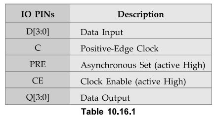
•
The equivalent VHDL code for a 4-bit register with a positive edge clock,
asynchronous set and clock enable is as follows.
LIBRARY
IEEE;
USE
IEEE.std_logic_1164.all;
ENTITY
flop IS
PORT(
C, CE, PRE : IN std_logic;
D
: IN std_logic_vector (3 downto 0);
Q
: OUT std_logic_vector (3 downto 0));
END
flop;
ARCHITECTURE
archi OF flop IS
BEGIN
PROCESS
(C, PRE)
BEGIN
IF
(PRE = 'l') THEN
Q
< = “1111'';
ELSIF
(C'event and C=’1’)THEN
IF
(CE = ’T) THEN
Q
< = D;
END
IF;
END
IF;
END
PROCESS;
END
archi;
3. VHDL Code for an N-bit Register
•
Oftenly the registers of different sizes are required in logic circuits. So it
is advisable to write a VHDL code for a register in which number of bits of a
register can be changed easily. The number of bits in a register are decided by
number of flip-flops used to build a register. The code discussed in the
previous section, i.e. code for a 4-bit register is modified by a parameter
that sets the number of flip-flops. This code is given below.
•
Here, we are using N as a parameter which is an integer called in VHDL as
GENERIC.
•
Here, the assignment operator (:=) is used to set the value of N to 16. A
register of any number of bits can be obtained just by changing this parameter.
Since the code is written for N-bit register, the D and Q signals are also
defined interms of N. The OTHERS => 'O' statement assigns a 'O' to each bit
of Q.
LIBRARY
IEEE;
USE
IEEE.std_logic_1164.all;
ENTITY
regN IS GENERIC(N:INTEGER : = 16);
PORT(D
: IN STD_LOGIC_VECTOR(N-1 DOWNTO 0);
Resetn,Clock
: IN STD_LOGIC;
Q
: OUT STD_LOGIC_VECTOR(N-1 DOWNTO 0));
END
regN;
ARCHITECTURE
Behavior OF regN IS
BEGIN
PROCESS(Resetn,
Clock)
BEGIN
IF
Resetn='0'THEN
Q<=(OTHERS=>
'0');
ELSIF
Clock'EVENT AND Clock = T THEN
Q<=D;
END
IF;
END
PROCESS;
END
Behavior;
4. VHDL Code for a Shift Register
a.
Using Sequential Statements
•
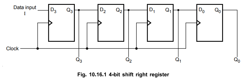
Fig. 10.16.1 shows a 4-bit shift right register.
•
The VHDL code for this register is given below. Here, the shift register is
described using sequential statements. Because of the WAIT-UNTIL statement, any
signal that is assigned a value inside the process has to be implemented as the
output of the flip-flop.
LIBRARY
IEEE;
USE
IEEE.std_logic_1164.all;
ENTITY
shiftreg IS
PORT(Clock
: IN STD_LOGIC;
I
: IN STD_LOGIC;
Q
: BUFFER STD_LOGIC_VECTOR (3 DOWNTO 0));
END
shiftreg;
ARCHITECTURE
Behavior OF shiftreg IS
BEGIN
PROCESS
BEGIN
WAIT
UNTIL clock'EVENT AND Clock = 1';
Q(0)<=
Q(l);
Q(l)<=
Q(2);
Q(2)<
= Q(3);
Q(3)<
= I;
END
PROCESS;
END
Behavior;
•
It is to be noted that in this VHDL code, the lines which perform the shift
operation can be written in reverse order i.e. Q(3) <= I as the first and
Q(0) <= Q(l) as the last line. The code produces the same circuit with any
sequence of these four lines. The reason is that due to the semantics of the
process statement, all of the statements inside the process are evaluated
separately and values are assigned to Q(0), Q(l), Q(2) and Q(3).
b.
Hierarchical Code for a 4-bit Shift Register
•
As shown in Fig. 10.16.1, 4-bit shift register consists of four D-flip-flops.
Each D-flip-flop can be considered as a subdrcuit. CAD system generally
includes libraries of prebuilt subcircuits. A good example of a library of
macrofunctions is the Library of Parameterized Modules (LPM) which is included as part of the MAX + plus II CAD
system. Each module in the library can be used in different ways, i.e.
parameterized and also technology independent. The LPM includes subcircuits
that have flip-flops. The predefined subcircuits in the LPM library can be
instantiated in VHDL code.
•
In the hierarchical code for a 4-bit shift register, we can use D flip-flop as
a subcircuit and 4 stages of it can be instantiated. The code is given below.
Here we are using VHDL construct PORT MAP to assign signal names to the ports
of a D flip-flop.
LIBRARY
IEEE;
USE
IEEE.std_logic_1164.all;
ENTITY
shiftreg IS
PORT(Clock
: IN STD_LOGIC
I
: IN STD_LOGIC
Q
: BUFFER STD_LOGIC_VECTOR(3 DOWNTO 0));
END
shiftreg;
ARCHITECTURE
Structure OF shiftreg IS
COMPONENT
DFF
PORT(D,Clock
: IN STDLOGIC;
Q
: OUT STD_LOGIC);
END
COMPONENT;
BEGIN
Stage3
: DFF PORT MAP (I, Clock, Q(3));
Stage2
: DFF PORT MAP (Q(3), Clock, Q(2));
Stage1
: DFF PORT MAP (Q(2), Clock, Q(l));
Stage0
: DFF PORT MAP (Q(l), Clock, Q(0));
END
Structure;
c.
VHDL Code for an n-bit Left-to-Right Shift Register
•
We can write the VHDL code for an n-bit left to right shift register by using
the GENERIC parameter n. The VHDL code is given below. Here, we have taken n =
16, but we can set size of the shift register to any number of bits. Here we
have taken parallel input P(bits ... P3P2P1P0) for loading data into the
register in parallel. Remaining code is same as the code for 4-bit shift
register with two exceptions. First is, P and output Q are to be given interms
of n. Second is, the ELSE clause which describes the shift right operation is
generalized to work for n number of flip-flops.
•
The 'Load' signal is used to control two operations. When 'Load' signal is 1,
the data is loaded in parallel into the register; otherwise the shift
left-to-right operation takes place.
LIBRARY
IEEE;
USE
IEEE.std_logic_1164.all;
ENTITY
sftregn IS GENERIC (n : INTEGER := 16);
PORT
( P : IN STD_LOGIC_VECTOR(n-l DOWNTO 0);
Clock : IN STD_LOGIC ;
Load,I
: IN STD_LOGIC;
Q
: BUFFER STD_LOGIC_VECTOR (n-1 DOWNTO
0));
END
sftregn;
ARCHITECTURE
Behavior OF sftregn IS
BEGIN
PROCESS
BEGIN
WAIT
UNTIL Clock'EVENT AND Clock = 1'; IF Load = '1' THEN
Q<=P;
ELSE
Genbits:FOR
i IN 0 TO n-2 LOOP
Q(i)
<= Q(i+1);
END
LOOP;
Q(n-l)<=I;
END
IF;
END
PROCESS;
END
Behavior;
d.
VHDL Code for a Left-to-Right Shift Register with an Enable Input
•
This code is same as the code given in the previous section with an exception
of an enable input, EN. When 'EN' signal is 1, the shift register behaves in the
same way as the normal left-to-right shift register. If 'EN' signal is 0, the
shift operation does not take place. That is, 'EN' equals to 0 prevents the
contents of the shift register from changing. The VHDL code for such a register
is given below.
LIBRARY
IEEE;
USE
IEEE.std_logic_1164.all;
-left-to-right
shift register with parallel load and enable
ENTITY
sftregne IS
GENERIC(n:INTEGER:
= 16);
PORT(P
: IN STD_LOGIC_VECTOR(n-l DOWNTO 0);
Load,
EN, I : IN STDLOGIC ;
Clock : IN STD_LOGIC ;
Q
: BUFFER STD_LOGIC_VECTOR (n-1 DOWNTO 0));
END
sftregne;
ARCHITECTURE
Behavior OF sftregne IS BEGIN
PROCESS
BEGIN
WAIT
UNTIL Clock'EVENT AND Clock = 1';
IF
EN = '1' THEN
IF
Load = 'I' THEN
Q
< = P;
ELSE
Genbits:FOR
i IN 0 TO n-2 LOOP
Q(i)<=
Q(i+1);
END
LOOP;
Q(n-l)<=I;
END
IF;
END
IF;
END
PROCESS;
END
Behavior;
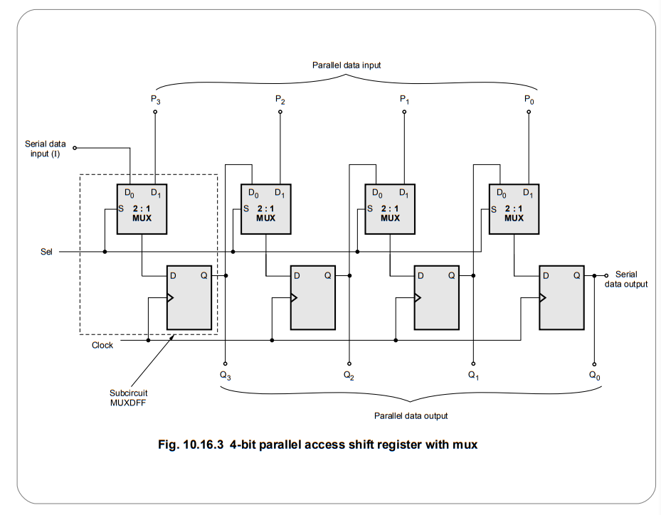
5. VHDL Code for a 4-bit Parallel Access Shift Register
a.
Using Sequential Statements
•
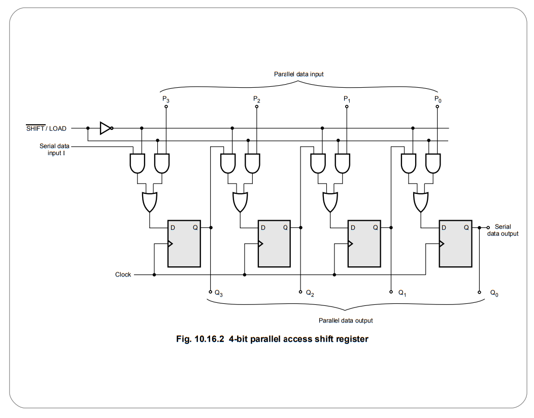
A 4-bit parallel access shift register is shown in Fig. 10.16.2.
•
The VHDL code for this shift register is given below.
•
When a positive edge clock signal is applied, if 'Load' signal is 1, then the
parallel input data, P is loaded into the shift register and same is obtained
at the output Q; otherwise the shift-right operation takes place, i.e. the
value of Q1 is shifted into the flip-flop with output Q0,
value of Q2 is shifted into Q1 value of Q3 is
shifted into Q2 and the value of serial input, I is shifted into Q3.
LIBRARY
IEEE;
USE
IEEE. std_logic_1164.all;
ENTITY
sftreg4 IS
PORT
( P : IN STD_LOGIC_VECTOR(3 DOWNTO 0);
Clock : IN STD_LOGIC;
Load,I
: IN STDLOGIC;
Q
: BUFFER STD_LOGIC_VECTOR(3 DOWNTO 0));
END
sftreg4;
ARCHITECTURE
Behavior OF sftreg4 IS
BEGIN
PROCESS
BEGIN
WAIT
UNTIL Clock'EVENT AND Clock = 1';
IF
Load = 'l'THEN
Q<=P;
ELSE
Q(0)<=
Q(l);
Q(l)<
= 0(2);
Q(2)<=
Q(3);
Q(3)<
= I;
END
IF;
END
PROCESS;
END
Behavior;
b.
Hierarchical Code for a 4-bit Parallel Access Shift Register
•
In a hierarchical code, we are taking D flip-flop with 2-to-l multiplexer as a
subcircuit. So four instantiations of such subdrcuits are needed. We are
calling this subcircuit as MUXDFF as shown in Fig. 10.16.3. The VHDL code for
this subcircuit is given here. There are two data inputs, DQ and Dp They are
selected using Sel input. The process statement specifies that on positive
clock edge, if sel is 0, then Q is assigned the value of DQ; otherwise Q is
assigned the value of DI.
LIBRARY
IEEE;
USE
IEEE.std_logic_1164.all;
ENTITY
MUXDFF IS
PORT
(DO, DI, Sel, Clock : IN STD LOGIC;
Q
: OUT STD_LOGIC);
END
MUXDFF;
ARCHITECTURE
Behavior OF MUXDFF IS
BEGIN
PROCESS
BEGIN
WAIT
UNTIL Clock'EVENT AND Clock = 1';
IF
Sel = O' THEN
Q<=D0;
ELSE
Q<=D1;
END
IF;
END
PROCESS;
END
Behavior;
•
The hierarchical code is given below. Four stages of the subcircuit MUXDFF are
instantiated in this code. The stage3 instantiates the leftmost subcircuit
MUXDFF having output Q3 and the stage0 instantiates the rightmost subcircuit
MUXDFF having output Q0.
•
When 'Load' signal is 1, data is loaded in parallel from the P input. When
'Load' signal is 0, shift right operation takes place as discussed earlier.
LIBRARY
IEEE;
USE
IEEE.std_logic_1164.all;
ENTITY
sftreg4 IS
PORT
(P : IN STD_LOGIC_VECTOR(3 DOWNTO 0);
Load,I,Clock
: IN STDLOGIC;
Q
: BUFFER STD_LOGIC_VECTOR (3 DOWNTO 0));
END
sftreg4;
ARCHITECTURE
Structure OF sftreg4 IS
COMPONENT
MUXDFF
PORT
(DO, DI, Sel, Clock : IN STD_LOGIC;
Q
: OUT STD_LOGIC);
END
COMPONENT;
BEGIN
Stage3
: MUXDFF PORT MAP (I, P(3), Sel, Clock, Q(3));
Stage2
: MUXDFF PORT MAP (Q(3), P(2), Sel, Clock, Q(2));
Stagel
: MUXDFF PORT MAP (Q(2), P(l), Sel, Clock, Q(l));
StageO
: MUXDFF PORT MAP (Q(l), P(0), Sel, Clock, Q(0));
END
Structure;
6. 8-bit Shift-Left Register with Positive-Edge Clock,
Asynchronous Parallel Load, Serial IN, and Serial OUT
•
The pin description of 8-bit shift-left register is as shown in the Table
10.16.2
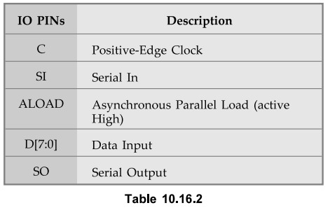
•
The VHDL code for an 8-bit shift-left register with a positive-edge clock,
asynchronous parallel load, serial in, and serial out is as follows.
LIBRARY
IEEE;
USE
IEEE.std_logic_1164.all;
ENTITY
shift IS
PORT(C,
SI, ALOAD : IN stdjogic;
D
: IN std_logic_vector(7 downto 0);
SO
: OUT stdjogic);
END
shift;
ARCHITECTURE
archi OF shift IS
signal
tmp: std_logic_vector(7 downto 0);
BEGIN
PROCESS
(C, ALOAD, D)
BEGIN
IF
(ALOAD='l’) THEN
tmp
<= D;
ELSIF
(C'event and C=T) THEN
tmp
< = tmp(6 downto 0) & SI;
END
IF;
END
PROCESS;
SO
< = tmp(7);
END
archi;
7. 8-bit Shift-Left Register with Positive-Edge Clock, Synchronous Parallel Load, Serial IN, and Serial OUT
• The pin description of 8-bit shift-left register is as shown in the Table 10.16.3
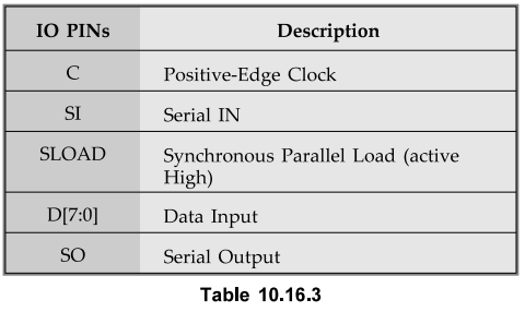
•
The VHDL code for an 8-bit shift-left register with a positive-edge clock,
synchronous parallel load, serial in, and serial out is as follows.
LIBRARY
IEEE;
USE
IEEE.std_logic_1164.all;
ENTITY
shift IS
PORT(
C, SI, SLOAD : IN stdjogic;
D
: IN std_logic_vector(7 downto 0);
SO
: OUT stdjogic);
END
shift;
ARCHITECTURE
archi OF shift IS
signal
tmp: std_logic_vector(7 downto 0);
BEGIN
PROCESS
(C)
BEGIN
IF
(C'event and C=’l') THEN
IF
(SLOAD=’l’) THEN
tmp
<= D;
ELSE
tmp
< = tmp(6 downto 0) & SI;
END
IF;
END
IF;
END
PROCESS;
SO
<= tmp(7);
END
archi;
8. 8-bit Shift-Left/Shift-Right Register with Positive-Edge
Clock, Serial IN, and Parallel OUT
•
The pin description of 8-bit shift-left/shift-right register is as shown in the
Table 10.16.4.
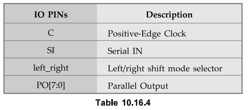
•
The VHDL code for an 8-bit shift-left/shift-right register with a positive-edge
clock, serial in, and serial out is as follows.
LIBRARY
IEEE;
USE
IEEE.std_logic_1164.all;
ENTITY
shift IS
PORT(C,
SI. left_right : IN std_logic;
PO
: OUT std_logic_vector(7 downto 0));
END
shift;
ARCHITECTURE
archi OF shift IS
signal
tmp: std_logic_vector(7 downto 0);
BEGIN
PROCESS
(C)
BEGIN
IF
(C’event and C=’l’) THEN
IF
(left_right='O') THEN
tmp
< = tmp(6 downto 0) & SI;
ELSE
tmp
< = SI & tmp(7 downto 1);
END
IF;
END
IF;
END
PROCESS;
PO
<= tmp;
END
archi;
9. VHDL Code for Universal Shift Register
•
Let us consider a universal shift register with four control modes as shown in
Fig. 10.16.4 Table 10.16.5 shows action to be performed by universal shift
register in different modes.

VHDL
CODE
library
IEEE;
Use
IEEE.std_logic_1164.all; entity usr is
generic
(n : NATURAL : = 8);
port
(a : in std_logic_vector (n-1) downto 0);
Left_in,
Right_in : in stdlogic ;
s
: in std_logic_vector (1 downto 0);
Clk,
reset : in std_logic;
q
= out std_logic_vector (n-1 downto 0));
end
entity usr;
architecture
rtl of usr is
begin
P0
: process (Clk, reset) is
variable
reg : std_logic_vector (n-1 downto 0);
begin
if
(reset = '0') then
reg
: = (others => '0');
elsif
risingedge (Clk) then
case
s is
when
"11" => reg : = a;
when
"10" = > reg : = reg (n-2 downto 0) and left_in ;
when
"01" => reg : Right_in & reg (n-1) downto 1);
when
others = > null;
end
case;
end
if;
q
< = reg;
end
process P0 ;
end
architecture rtl ;
Review Questions
1. Write a VHDL code for shift register.
2. Write a VHDL code for a 4-bit universal shift register.
Digital Logic Circuits: Unit V: VHDL : Tag: : - VHDL Code for Registers
Related Topics
Related Subjects

Digital Logic Circuits
EE3302 3rd Semester EEE Dept | 2021 Regulation | 3rd Semester EEE Dept 2021 Regulation