Physics for Electrical Engineering: Unit III: Semiconductors and Transport Physics
Carrier concentration in intrinsic semiconductors
Definition, Energy band diagram, derivation, equation
In general, the number of charge carriers per unit volume of the material is called carrier concentration. It is also known as density of charge carriers.
CARRIER CONCENTRATION IN INTRINSIC SEMICONDUCTORS
Definition
The
number of electrons in conduction band per unit volume of the material is
called as electron concentration (n).
Similarly
the number of holes in valence band per unit volume of the material is called
hole concentration (p).
In
general, the number of charge carriers per unit volume of the material is
called carrier concentration. It is also known as density of charge carriers.
Density
of Electrons in Conduction Band (Derivation)
The
number of electrons per unit volume in conduction band for energy between E and
E+ dE is given by
dn
= Z (E) F (E) dE ...(1)
where
Z (E) dE - Density of states in energy between E and E+ dE
F
(E) - Probability of electron occupancy.
Number
of electrons in conduction band for the entire range is calculated by
integrating eqn (1) between energy Ec and + ∞.
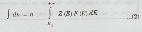
Ec
is energy corresponding to the bottom most level and +∞ is energy corresponding
to the upper most level in conduction band. (Fig 3.5).

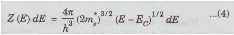
Density
of states in conduction band between the energy range E and E+ dE is given by
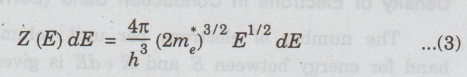
The
bottom edge of the conduction band (EC) denotes the potential energy
of an electron at rest. Therefore, (E - EC) is the kinetic energy of
conduction electron at higher energy levels.
Thus,
in eqn (3), E is replaced as (E - EC)
The
electrons in conduction band are not totally free. They move in a periodic
potential of the crystal lattice. Therefore, in eqn (3), the mass of the
electron (m) is replaced by its effective mass m*e
according to band theory of solids.
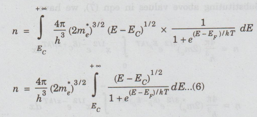
The
probability of electron occupation is given by Fermi distribution function
F
(E) = 1 / 1 + e(E-EF)/kT ...(5)
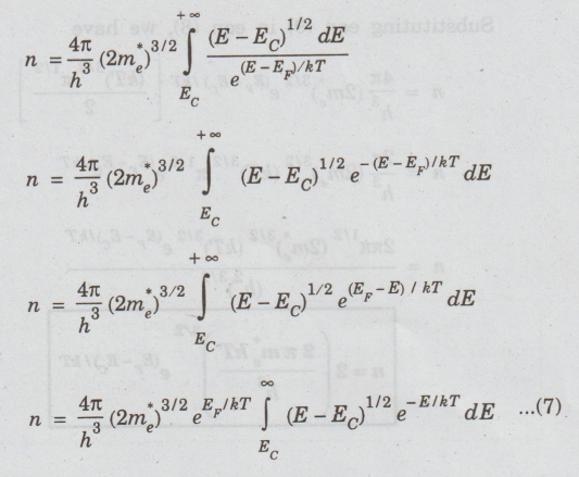
Substituting
eqns (4) and (5) in (2), we get
Since
kT is very small and (E - EF) is greater than kT, (E – EF)/kT
is very large compared to '1' Hence, '1' from the denominator of eqn (6) is
neglected.
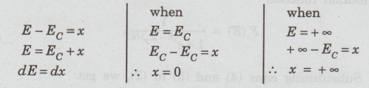
To
evaluate above integral in eqn (7), let us assume
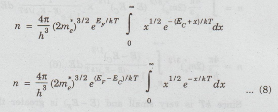
Substituting
above values in eqn (7), we have
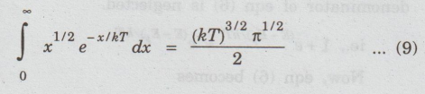
Using
the gamma function, it is shown that
Substituting
eqn (9) in eqn (8), we have
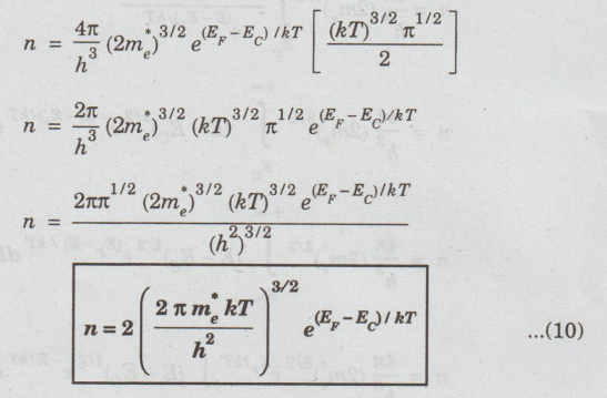
Equation
(10) is the expression for concentration of electrons in the conduction band of
intrinsic semiconductor.
Density
of holes in Valence Band of Intrinsic Semiconductor (Derivation)
We
know that if an electron is transferred from valence band to conduction band, a
hole is created in valence band.
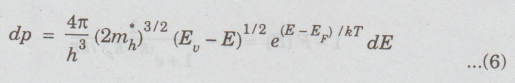
Let
dp be the number of holes per unit volume in valence band between the energy E
and E + dE.
dp
= Z (E) (1-F (E)) dE ...(1)
where
Z (E) dE → Density of states in the energy range E and E + dE.
Since
F (E) is the probability of electron occupation 1-F (E) is the probability of
an unoccupied electron state, i.e., probability of presence of hole,
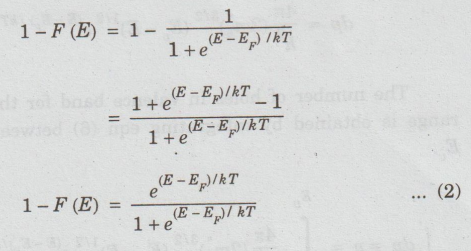
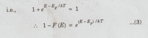
Since E is very small when compared to E in valence band, (E-E) is a negative quantity. Therefore, e (E - EF)/kT is very small and it is neglected in the denominator term of eqn (2).
Density
of states in valence band,
Here,
m is the effective mass of the hole in valence band.
EU’
top of energy level in valence band is the potential energy of a hole at rest.
Hence, (EU - E) is the kinetic energy of the hole at level below E.
So the term E in eqn (4) is replaced as (EU - E).
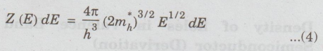
Z
(E) dE = 4π / h3 (2m*h)3/2 (EU – E)1/2
dE ...(5)
Substituting
eqns (3) and (5) in (1), we get
The
number of holes in valence band for the entire energy range is obtained by
integrating eqn (6) between limits - ∞ to EU.
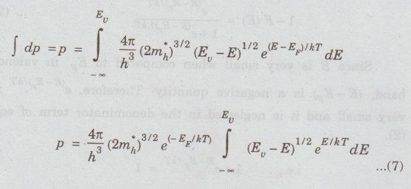
To
evaluate the integral in eqn (7), let us assume,
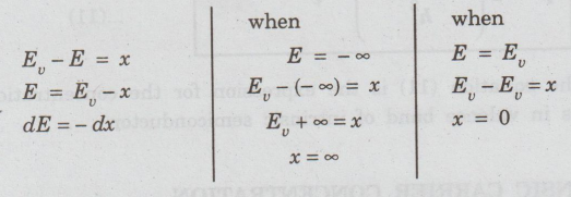
Substituting
these values in eqn (7), we have
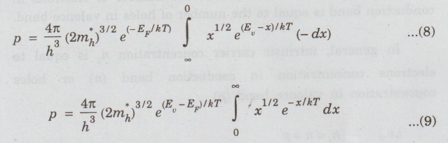
[-ve sign is omitted by interchanging the
limits]
Using
the gamma function, it is shown that

Substituting
eqn (10) in eqn (9), we have
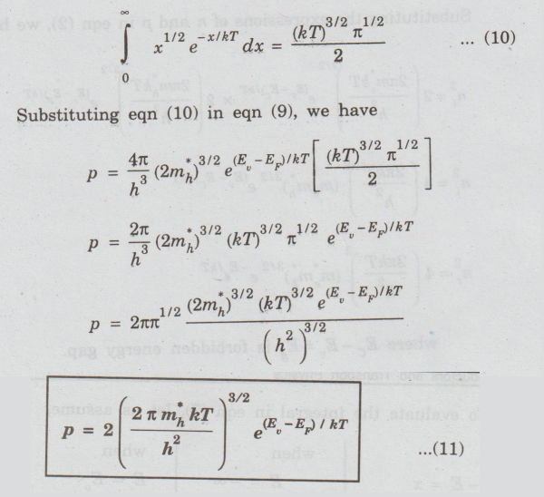
The
equation (11) is the expression for the concentration of holes in valence band
of intrinsic semiconductor.
Physics for Electrical Engineering: Unit III: Semiconductors and Transport Physics : Tag: : Definition, Energy band diagram, derivation, equation - Carrier concentration in intrinsic semiconductors
Related Topics
Related Subjects
Physics for Electrical Engineering
PH3202 2nd Semester 2021 Regulation | 2nd Semester EEE Dept 2021 Regulation