Physics for Electrical Engineering: Unit V: Nano Devices
Optics in Quantum structures
Nano Devices
Nanomaterials have attracted much attention due to their novel optical properties that are markedly different from bulk materials.
OPTICS IN QUANTUM STRUCTURES
Optical properties
Nanomaterials
have attracted much attention due to their novel optical properties that are
markedly different from bulk materials.
The
reason for this change in optical properties is due to the quantum confinement
of electrons in nanomaterials and surface plasma resonance.
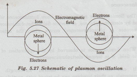
Surface Plasmon
Surface
plasmon is the natural oscillation of electron gas inside the nanosphere. It
can appear on the surface of bulk solids, thin films, and nanoparticles. On the
surface of bulk solids, surface plasmons appear as a propagating wave parallel
to the surface.
When
the nanosphere size is smaller than the wavelength of incident light, the
frequency of surface plasmon becomes comparable to the frequency of radiation
due to constructive interference. Then a resonance occurs and surface plasmon
resonance (SPR) is generated (Fig. 5.27).
Other Factors that Contribute to Optical Properties
Efficient
energy and charge transfer in nanoscale dimension further contribute to the
novel properties. Linear and nonlinear optical properties of the material can be
finely tuned by controlling their dimension and surface chemistry.
The
optical properties of nanomaterials depend on their size, shape, surface
characteristics, doping, and interaction with the surrounding environment or
other nanostructures.
A
change in size of the CdSe semiconductor nanoparticles alters their optical
properties. (A 2.3 nm CdSe emits blue light, whereas a 5.5 nm CdSe emits red
light) A change in the size of metal nanoparticles causes some change in their
optical properties.
Quantum Size Effect
Quantum
size effect is most significant in semiconductor nanoparticles. In
semiconductors, the bandgap energy is of the order of a few electron volts.
dia
As the size of the particle increases, absorption shifts towards the shorter
wavelength (blue shifts) indicates increase in the bandgap energy.
Luminescence
The
Semiconductor nanoparticles show luminescence when excited by electrons,
photons, or electric field. Photoluminescence (fluorescence or phosphorescence)
occurs when the external stimulus is due to photons.
When
luminescence is observed by the application of an electric field, it is termed
electroluminescence.
It
can be tuned to the desired wavelength for nanomaterials as their bandgap can
be tuned with particle size.
Nanomaterials
show high quantum efficiency for cathodoluminescence also, in which
luminescence is produced by electrons of very high energy incident on
materials.
Finally,
thermoluminescence is very strong for nanomaterials which have defect levels
and larger number of surface atoms that can act as efficient electron/hole
traps.
Optical Reflectance
Optical
reflectance is defined by the fraction of incident light reflected from the
surface of a material. Metals show high reflectance. It is due to the presence
of a partially filled conduction band. Thus, absorption and reflection of
photons take a continuum of energies from the infrared to visible region.
Semiconductors,
on the other hand, show low absorption and reflectance in infrared range and
increases drastically at the bandgap and increases further in the ultraviolet
region.
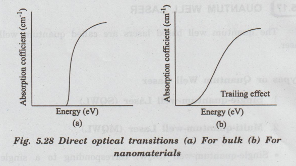
Direct
optical transitions for bulk and nanomaterials are shown in fig. 5.28.
Absorption edge of nanomaterials denotes trailing effect as compared to bulk
due to variation in density of states, surface restructuring and a random
distribution of impurities.
Applications Based on Optical Properties
There
are some fascinating applications of the optical properties of nanomaterials in
the areas of optical detectors, lasers, sensors, imaging, phosphors, displays,
solar cells, photocatalysis, photoelectrochemistry, and biomedicine. Some of
these applications are listed as follows.
1.
Suitable for optoelectronic materials such as switches, amplifiers, gratings,
splitters, isolators, lasers, and detectors
2.
Widely used in polymers to increase their refractive index, which makes them
suitable as optical components
3.
Useful in preparing abrasion-resistant coatings whose optical clarity can be
enhanced
4.
Nanoparticles in castings improve shielding against electromagnetic fields in
computers
5.
LCDs and organic LEDs developed using nanomaterials show better resolution of
images.
Physics for Electrical Engineering: Unit V: Nano Devices : Tag: : Nano Devices - Optics in Quantum structures
Related Topics
Related Subjects
Physics for Electrical Engineering
PH3202 2nd Semester 2021 Regulation | 2nd Semester EEE Dept 2021 Regulation