Digital Logic Circuits: Unit V: VHDL
RTL Design
VHDL
• Register Transfer Level, or RTL design lies between a purely behavioral description of the desired circuit and a purely structural one.
RTL Design
•
Register Transfer Level, or RTL design lies between a purely behavioral
description of the desired circuit and a purely structural one. An RTL
description describes a circuit's registers and the sequence of transfers
between these registers but does not describe the hardware used to carry out
these operations. The steps in RTL design are :
1.
Determine the number and sizes of registers needed to hold the data used by the
device,
2.
Determine the logic and arithmetic operations that need to be performed on
these register contents and
3.
Design a sequential circuit whose outputs control how the register contents are
updated in order to obtain the desired results.
•
Producing an RTL design is similar to writing a computer program in a
conventional programming language. Choosing registers is the same as choosing
variables. Designing the flow of data in the "datapath" is analogous
to writing expressions involving the variables (registers) and operators
(combinational functions). Designing the controller sequential circuit is
similar to deciding on the flow of control within the program (if/then/else,
while-loops, etc).
•
As a simple example, consider a device that needs to add four numbers. In VHDL,
given signals of the correct type, we can simply write :
s<=((a
+ b) + c) + d;
•
This particular description is simple enough that it can be synthesized. However,
the resulting circuit will be a fairly large combinational circuit comprising
three adder circuits as shown in Fig. 10.19.1.
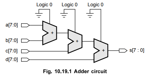
• A behavioral description, not being
concerned with implementation details, would be complete at this point.
However, if we were concerned about the cost of the implementation we might
decide to break down the computation into a sequence of steps, each one
involving only a single addition :
s
= 0;
s
= s + a ;
s
= s + b ;
s
= s + c ;
s
= s + d ;
•
Where each operation is executed sequentially. The logic required is now one
adder, a register to hold the value of s in-between operations, a multiplexer
to select the input to be added, and a circuit to clear s at the start of the
computation.
•
Although this approach only needs one adder, the process requires more steps
and will take longer time. Circuits that divide up a computation into a
sequence of arithmetic and logic operations are quite common and this type of
design is called Register Transfer Level (RTL) or "dataflow" design.
•
An RTL design is composed of :
1.
Registers and combinational function blocks (e.g. adders and multiplexers)
called the datapath and
2.
A finite sequential circuit, called the controller that controls the transfer
of data through the function blocks and between the registers.
•
In VHDL RTL design, the gate-level design and optimization of the datapath
(registers, multiplexers, and combinational functions) is done by the
synthesizer. However, the designer must design the sequential circuit and
decide which register transfers are performed in which state.
•
The RTL designer can trade off datapath complexity (e.g. using more adders and
thus using more chip area) against speed (e.g. having more adders means fewer
steps are required to obtain the result). RTL design is well suited for the
design of CPUs and special-purpose processors such as disk drive controllers,
video display cards, network adapter cards, etc. It gives the designer great
flexibility in choosing between processing speed and circuit complexity.
•
The Fig. 10.19.2 shows a generic component in the datapath. Each RTL design
will be composed of one of the following building blocks for each register. The
structure allows the contents of each register to be updated at the end of each
clock period with a value selected by the controller. The widths of the
registers, the types of combinational functions and their inputs will be
determined by the application. A typical design will include many of these
components.
Review Questions
1. Explain the design VHDL. procedure of RTL using VHDL.
AU : Dec.-l0, Marks 10
2. When can RTL be systems? used to represent digital
AU : May-11, Marks 2
3. Describe the RTL in VHDL.
AU : May-11, Marks 16
4. Explain in detail the design procedure for register transfer
language.
AU : Dec.-11, Marks 16
5. Express how arithmetic and logic operations are expressed
using RTL.
AU : Dec.-11, Marks 8
Digital Logic Circuits: Unit V: VHDL : Tag: : VHDL - RTL Design
Related Topics
Related Subjects

Digital Logic Circuits
EE3302 3rd Semester EEE Dept | 2021 Regulation | 3rd Semester EEE Dept 2021 Regulation