Digital Logic Circuits: Unit III: (a) Flip-Flops
Clocked JK Flip-Flop
Circuit diagram, Logic symbol, Truth table, Characteristic equation, IO Waveform
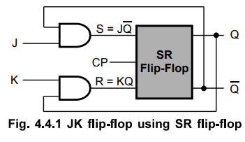
• The uncertainty in the state of an SR flip-flop when S = R = 1 can be eliminated by converting it into a JK flip-flop.
Clocked JK Flip-Flop
•
The uncertainty in the state of an SR flip-flop when S = R = 1 can be
eliminated by converting it into a JK flip-flop. The data inputs are J and K
which are ANDed with ![]() and Q, respectively, to obtain S and R inputs, as
shown in the Fig. 4.4.1. Thus,
and Q, respectively, to obtain S and R inputs, as
shown in the Fig. 4.4.1. Thus, 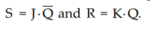 .
.
•
Let us see the operation of JK flip-flop.
Case
1 : J = K = 0
When
J = K = 0, S = R = 0 and according to truth table of SR flip-flop there is no
change in the output.
When
inputs J = K = 0, output does not change.
Case
2 : J = 1 and K = 0
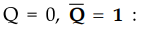 When J = 1, K = 0 and Q = 0, S = 1 and R = 0. According to truth table of SR
flip-flop it is set state and the output Q will be 1.
When J = 1, K = 0 and Q = 0, S = 1 and R = 0. According to truth table of SR
flip-flop it is set state and the output Q will be 1.
 When J = 1, K = 0 and Q = 1, S = 0 and R
= 0. Since SR = 00, there is no change in the output and therefore,
When J = 1, K = 0 and Q = 1, S = 0 and R
= 0. Since SR = 00, there is no change in the output and therefore, 
The
inputs J = 1 and K = 0, makes Q = 1, i.e. set state.
Case
3 : J = 0 and K = 1
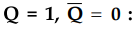
When J = 0, K = 1 and Q = 0, S = 0 and R
= 0. Since SR = 00, there is no change in the output and therefore, 
When J = 0, K = 1 and Q = 1, S = 0 and R
= 1. According to truth table of SR flip-flop it is a reset state and the
output Q will be 0.
The
inputs J = 0 and K = 1, makes Q = 0, i.e., reset state.
Case
4 : J = K = 1
When J = K = 1 and Q = 0, S = 1 and R =
0. According to truth table of SR flip-flop it is a set state and the output Q
will be 1.
When J = K = 1 and Q = 1, S = 0 and R =
1. According to truth table of SR flip-flop it is a reset state and the output
Q will be 0.
The
input J = K = 1, toggles the flip-flop output.
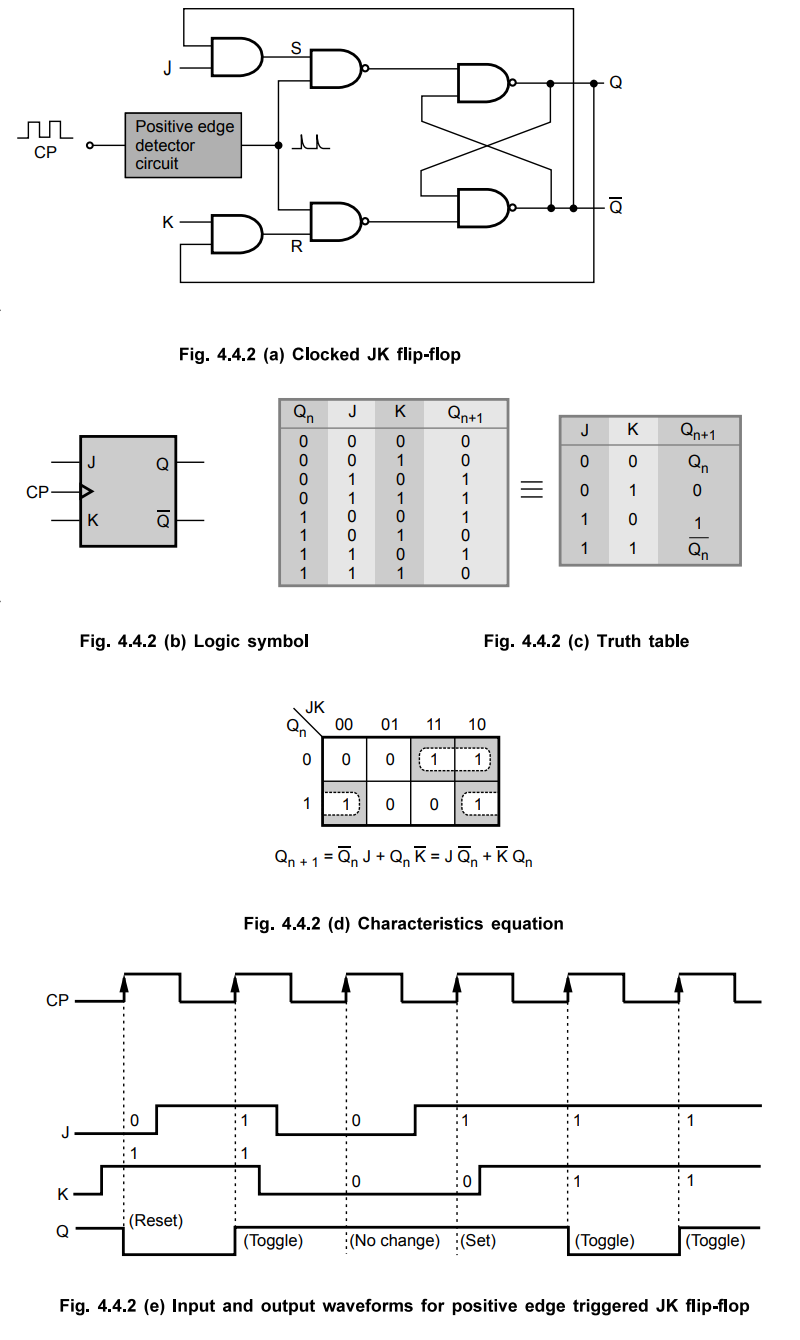
The
Fig. 4.4.2 shows the logic symbol, truth table and timing diagram of positive
edge triggered JK flip-flop.
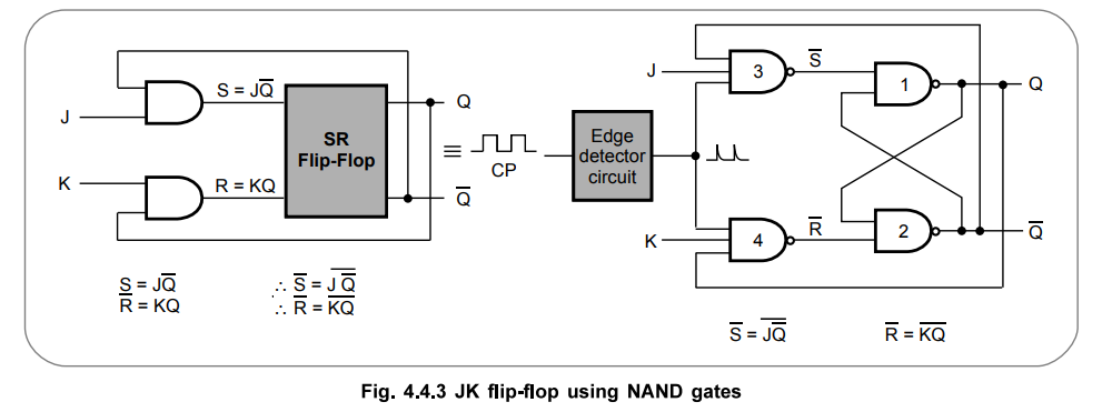
1. JK Flip-Flop using NAND Gates
•
In the previous section we have seen the operation of JK flip-flop using SR
flip-flop and AND gates. It is not necessary to use the AND gates of Fig. 4.4.2
(a), since the same function can be performed by adding an extra input terminal
to NAND gates 3 and 4 of Fig. 4.4.3. The Fig. 4.4.3 shows the modified circuit
of JK flip-flop which has only NAND gates.
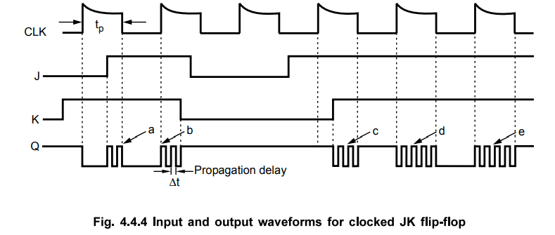
2. Race-around Condition
•
In JK flip-flop, when J = K = 1, the output toggles (output changes either from
0 to 1 or from 1 to 0). Consider that initially Q = 0 and J = K = 1. After a
time interval Δt equal to the propagation delay through two NAND gates in
series, the output will change to Q = 1 and after another time interval of At
the output will change back to Q = 0. This toggling will continue until the
flip-flop is enabled and J = K = 1. At the end of clock pulse the flip-flop is
disabled and the value of Q is uncertain. This situation is referred to as the
race-around condition. This is illustrated in Fig. 4.4.4. This condition exists
when tp ≥ Δt. Thus by keeping tp < Δt we can avoid
race around condition.
•
We can keep tp < At by keeping the duration of edge less than Δt. A more
practical method for overcoming this difficulty is the use of the Master-Slave
(MS) configuration.
Ex.
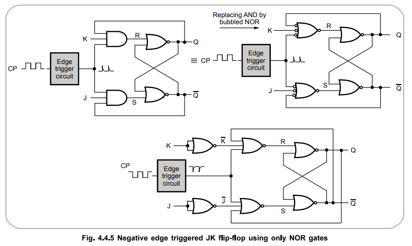
4.4.1 Realize a JK flip-flop using only NOR gates.
AU
: Dec.-03, Marks 8
Sol.
:
Review Questions
1. Draw the logic circuit of a clocked JK flip-flop.
2. Explain the working of JK flip-flop.
3. Sketch the truth table or state table for JK flip-flop.
4. With reference to a JK flip-flop, what is racing ?
5. How can race condition be avoided in flip-flop ?
6. What is race around condition and how is it overcome ?
Explain these concepts with relevant timing diagrams.
Digital Logic Circuits: Unit III: (a) Flip-Flops : Tag: : Circuit diagram, Logic symbol, Truth table, Characteristic equation, IO Waveform - Clocked JK Flip-Flop
Digital Logic Circuits: Unit III: (a) Flip-Flops
Under Subject

Digital Logic Circuits
EE3302 3rd Semester EEE Dept | 2021 Regulation | 3rd Semester EEE Dept 2021 Regulation
Related Subjects
Probability and complex function
MA3303 3rd Semester EEE Dept | 2021 Regulation | 3rd Semester EEE Dept 2021 Regulation

Electromagnetic Theory
EE3301 3rd Semester EEE Dept | 2021 Regulation | 3rd Semester EEE Dept 2021 Regulation
Digital Logic Circuits
EE3302 3rd Semester EEE Dept | 2021 Regulation | 3rd Semester EEE Dept 2021 Regulation

Electron Devices and Circuits
EC3301 3rd Semester EEE Dept | 2021 Regulation | 3rd Semester EEE Dept 2021 Regulation

Electrical Machines I
EE3303 EM 1 3rd Semester EEE Dept | 2021 Regulation | 3rd Semester EEE Dept 2021 Regulation
C Programming and Data Structures
CS3353 3rd Semester EEE, ECE Dept | 2021 Regulation | 3rd Semester EEE Dept 2021 Regulation