Digital Logic Circuits: Unit III: (a) Flip-Flops
SR Flip-Flop
Circuit diagram, Logic symbol, Truth table, Characteristic equation, IO Waveform
The circuit is similar to SR latch except enable signal is replaced by the Clock Pulse (CP) followed by the positive edge detector circuit.
SR Flip-Flop
AU:
Dec.-03, 05, 14, 15, May-04, 10, 12
Positive
Edge Triggered SR Flip-Flop
The
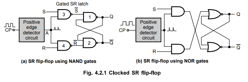
Fig. 4.2.1 shows the positive edge triggered clocked SR flip-flop. The circuit
is similar to SR latch except enable signal is replaced by the Clock Pulse (CP)
followed by the positive edge detector circuit. The edge detector circuit is a
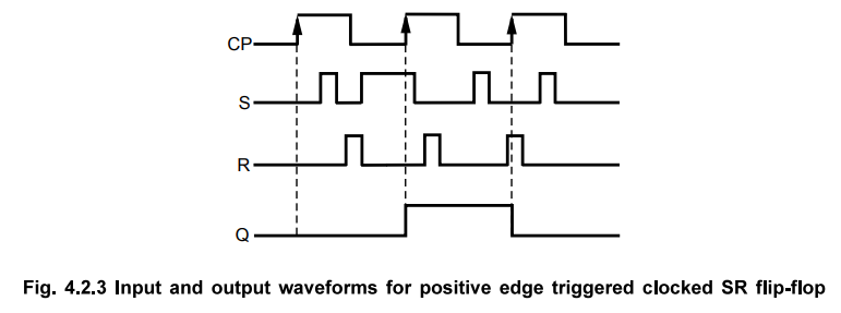
differentiator. The Fig. 4.2.3 shows input and output waveforms for positive
edge triggered clocked SR flip-flop. As shown in Fig. 4.2.3 the circuit output
responds to the S and R inputs only at the positive edges of the clock pulse.
At any other instants of time, the SR flip-flop will not respond to the changes
in input.
The
Fig. 4.2.2 shows the logic symbol and truth table of clocked SR flip-flop.
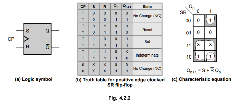
Case
1:
If S = R = 0 and the clock pulse is applied, the output do not change, i.e. Qn+
1 = Q. This is indicated in the first row of the truth table.
Case
2:
If S = 0, R = 1 and the clock pulse is applied, Qn + 1 = 0 . This is
indicated in the second row of the truth table.
Case
3 : If
S = 1, R= 0 and the clock pulse is applied, Qn + 1 = 1. This is
indicated in the third row of the truth table.
Case
4: If
S = R = 1 and the clock pulse is applied, the state of the flip-flip is
undefined and therefore is indicated as indeterminate in the fourth row of the
truth table.
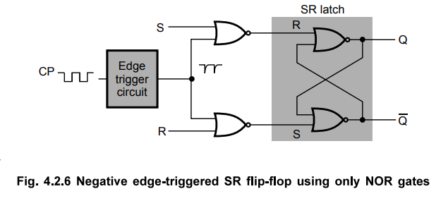
Negative
Edge Triggered SR Flip-Flop
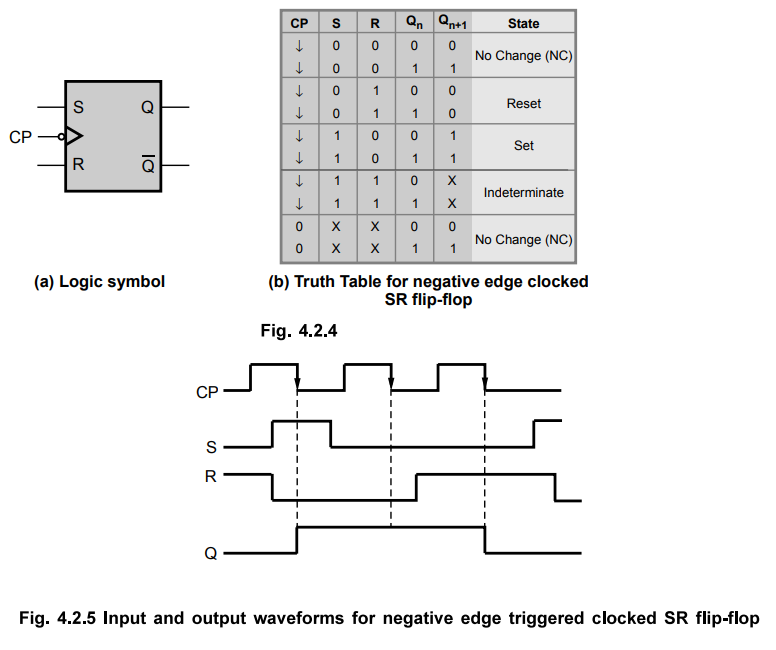
In
the negative edge triggered SR flip-flop, the negative edge detector circuit is
used and the circuit output responds at the negative edges of the clock pulse.
The Fig. 4.2.4 and Fig. 4.2.5 shows the logic symbol, truth table and input and
output waveforms for negative edge triggered SR flip-flop. The bubble at the
clock input indicates that the flip-flop is negative edge triggered.
Ex.
4.2.1 Realize SR flip-flop using NOR gates.
Sol.
:
Review Questions
1. Draw the circuit for SR flip-flop.
2. Realize SR flip-flop using NOR gates and explain its
operation.
3. Derive the characteristic equation of a SR flip-flop.
4. Realize a SR flip-flop using NAND gates and explain its
operation.
5. Explain the circuit of a SR flip-flop and explain its
operation.
6. Draw the truth table and state diagram of SR flip-flop.
Digital Logic Circuits: Unit III: (a) Flip-Flops : Tag: : Circuit diagram, Logic symbol, Truth table, Characteristic equation, IO Waveform - SR Flip-Flop
Digital Logic Circuits: Unit III: (a) Flip-Flops
Under Subject

Digital Logic Circuits
EE3302 3rd Semester EEE Dept | 2021 Regulation | 3rd Semester EEE Dept 2021 Regulation
Related Subjects

Probability and complex function
MA3303 3rd Semester EEE Dept | 2021 Regulation | 3rd Semester EEE Dept 2021 Regulation

Electromagnetic Theory
EE3301 3rd Semester EEE Dept | 2021 Regulation | 3rd Semester EEE Dept 2021 Regulation
Digital Logic Circuits
EE3302 3rd Semester EEE Dept | 2021 Regulation | 3rd Semester EEE Dept 2021 Regulation

Electron Devices and Circuits
EC3301 3rd Semester EEE Dept | 2021 Regulation | 3rd Semester EEE Dept 2021 Regulation

Electrical Machines I
EE3303 EM 1 3rd Semester EEE Dept | 2021 Regulation | 3rd Semester EEE Dept 2021 Regulation

C Programming and Data Structures
CS3353 3rd Semester EEE, ECE Dept | 2021 Regulation | 3rd Semester EEE Dept 2021 Regulation