Digital Logic Circuits: Unit III: (a) Flip-Flops
D Flip-Flop
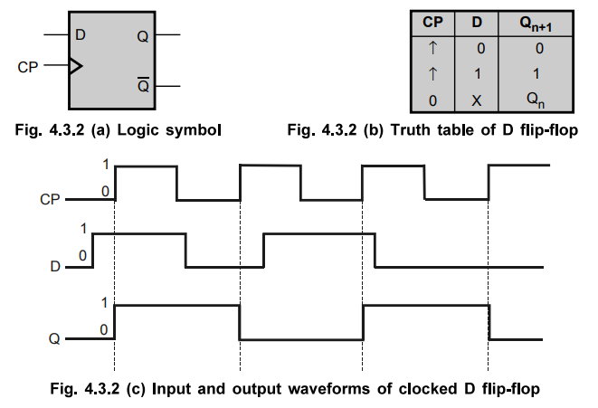
Circuit diagram, Logic symbol, Truth table, Characteristic equation, IO Waveform
The SR flip-flop has two data inputs S and R. The S input is made high to store 1 in the flip-flop and R input is made high to store 0 in the flip-flop.
D Flip-Flop
•
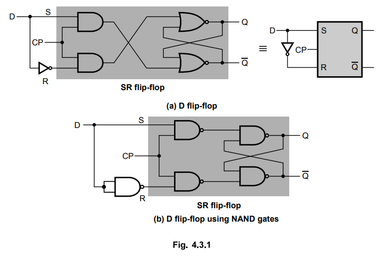
The Fig. 4.3.1 shows the logic diagrams of D flip-flop. The basic building
block of D flip-flop is a SR flip-flop. The SR flip-flop has two data inputs S
and R. The S input is made high to store 1 in the flip-flop and R input is made
high to store 0 in the flip-flop.
•
Looking at the truth table of the SR flip-flop we can realize that when both
inputs are same the output either does not change or it is invalid (Inputs 00,
no change and inputs 11, invalid). In many practical applications, these input
conditions are not required. These input conditions can be avoided by making
them complement of each other. This modified SR flip-flop is known as D
flip-flop.
•
As shown in the Fig. 4.3.1, the D input goes directly to the S input, and its
complement is applied to the R input. Due to these connections, only two input
conditions exists, either S= 0 and R = 1 or S = 1 and R = 0. The truth table
for D flip-flop consider only these two conditions and it is as shown in the
Fig. 4.3.2 (b).
•
Looking at the truth table for D flip-flop we can realize that Qn +1
function follows D input at the positive going edges of the clock pulses. Hence
the characteristic equation for D flip-flop is Qn +1 = D. However,
the output Q n +1 is delayed by one clock period. Thus, D flip-flop
is also known as delay flip-flop.
•
If we connect the ![]() output of D flip-flop to its D input as shown in
the Fig. 4.3.3, the output of D flip-flop will change either from 0 to 1 or
from 1 to 0 at every positive edge of the D flip-flop.
output of D flip-flop to its D input as shown in
the Fig. 4.3.3, the output of D flip-flop will change either from 0 to 1 or
from 1 to 0 at every positive edge of the D flip-flop.

•
Such change in the output is known as toggling of the flip-flop output.
Negative
Edge Triggered D Flip-Flop
•
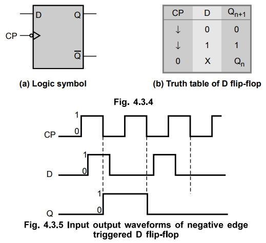
In the previous explanation we have seen the output of D flip-flop is sensitive
at the positive edge of the clock input. In case of negative edge triggering,
the output is sensitive at the negative edge of the clock input. The Fig. 4.3.4
shows the logic symbol and truth table for negative edge triggered D flip-flop
and Fig. 4.3.5 shows input and output waveforms for negative edge triggered D
flip-flop. The bubble at the clock input indicates that the flip-flop is negative
edge triggered.
Review Questions
1. Give the truth table I state table for D flip-flop.
2. Draw and explain the working of clocked D flip-flop.
Digital Logic Circuits: Unit III: (a) Flip-Flops : Tag: : Circuit diagram, Logic symbol, Truth table, Characteristic equation, IO Waveform - D Flip-Flop
Related Topics
Related Subjects

Digital Logic Circuits
EE3302 3rd Semester EEE Dept | 2021 Regulation | 3rd Semester EEE Dept 2021 Regulation