Digital Logic Circuits: Unit III: (a) Flip-Flops
Introduction to Sequential Logic Circuit
• There are many applications in which digital outputs are required to be generated in accordance with the sequence in which the input signals are received.
Introduction to Sequential Logic Circuit
May-05, Dec.-14, 15, 17, 18
•
There are many applications in which digital outputs are required to be
generated in accordance with the sequence in which the input signals are
received. This requirement cannot be satisfied using a combinational logic
system. These applications require outputs to be generated that are not only
dependent on the present input conditions but they also depend upon the past
history of these inputs. The past history is provided by feedback from the
output back to the input.
•
Fig. 4.1.1 shows the block diagram of sequential drcuit/Finite State Machine
(FSM). As shown in the Fig. 4.1.1, memory elements are connected to the
combinational circuit as a feedback path.

•
The information stored in the memory elements at any given time defines the
present state of the sequential circuit. The present state and the external
inputs determine the outputs and the next state of the sequential circuit. Thus
we can specify the sequential circuit by a time sequence of external inputs,
internal states (present states and next states), and outputs. The counters and
registers are the common examples of sequential circuits.
The
memory element used in sequential circuits is a flip-flop which is capable of
storing 1-bit binary information.
1. Comparison between Combinational and Sequential Logic Circuits

2. Clock
•
A clock signal is a particular type of signal that oscillates between a high
and a low state and is utilized to co-ordinate actions of circuits. It is
produced by a clock generator. The most common clock signal is in the form of a
square wave with a 50 % duty cycle, usually with a fixed, constant frequency as
shown in Fig. 4.1.2.
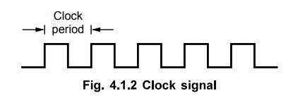
Circuits
using the clock signal for synchronization may become active at either the
rising edge, falling edge or in the case of double data rate, both in the
rising and in the falling edges of the clock cycle.
•
The time required to complete one cycle is called 'clock period' or 'clock
cycle'. Ideally, the clock signal should have sharp transitions from one level
to other as shown in Fig. 4.1.2.
3. Types of Triggering
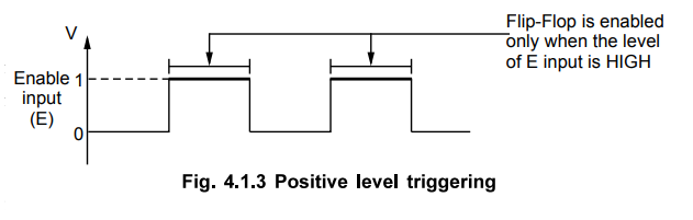
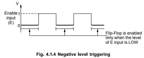
Level
Triggering
•
In the level triggering, the output state is allowed to change according to
input(s) when active level (either positive or negative) is maintained at the
enable input. There are two types of level triggered latches :
•
Positive level triggered : The output Enable 1 of flip-flop
responds to the input input changes only when its enable input is 0 1 (HIGH).
•
Negative level triggered : The output of flip-flop responds
to the input changes only when its enable input is 0 (LOW).
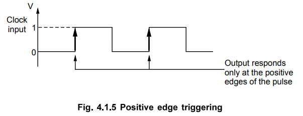
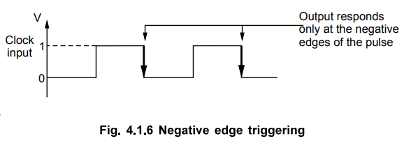
Edge
Triggering
•
In the edge triggering, the output responds to the changes in the input only at
the positive or negative edge of the clock pulse at the clock input. Edge
triggered flip-flops are designed to avoid race condition. There are two types
of edge triggering.
•
Positive edge triggering : Here, the output responds to the
changes in the input only at the positive edge of the clock pulse at the clock
input.
•
Negative edge triggering : Here, the output responds to the changes
in the input only at the negative edge of the clock pulse at the clock input.
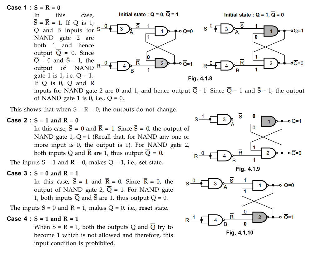
4. SR Latch
•
Fig. 4.1.7 shows RS latch which is 1-bit memory cell. As S (Set) shown in the
Fig. 4.1.7, two inverters 3 and 4 are connected to enter the digital
information. Input for gate 3 is S and input for gate 4 is R. This latch is
also called RS latch.
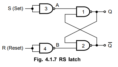
•
For understanding the circuit operation, we must first is logic 0 and
accordingly we have to determine the output of other NAND gate in the cross
coupled circuit. Because the output of NAND gate is 1 if any one input is 0.
The circuit operation is as follows. In Fig. 4.1.8, the output of shaded NAND
gate is determined first, and the 0 input that decides the output of shaded
NAND as 1 is shown in bold.
5. Gated SR Latch
• In the SR latch we have seen that output changes occur immediately after the input changes occur i.e. the latch is sensitive to its S and R inputs at all times. However, it can easily be modified to create a latch that is sensitive to these inputs only when an enable input is active. Such a latch with enable input is known as gated SR latch. It is as shown in the Fig. 4.1.11. The Table 4.1.2 shows the truth table for gated latch. As shown by truth table, the circuit behaves like a SR latch when EN = 1, and retains its previous state when EN = 0.

6. Latches Vs Flip-Flops
•
Latches and flip-flops are the basic building blocks of the most sequential
circuits. The main difference between latches and flip-flops is in the method
used for changing their state.
•
A simple latch forms the basis for the flip-flop. Latches are controlled by
enable signal, and they are level triggered, either positive level triggered or
negative level triggered. The output state is free to change according to the S
and R input values, when active level is maintained at the enable input.
Flip-flops are different from latches. Flip-flops are pulse or clock edge
triggered instead of level triggered.
Review Questions
1. Define sequential
logic circuit.
2. What is flip-flop?
3. Give the comparison
between combinational and sequential logic circuits.
4. What is clock?
State its use.
5. Explain the
different types of triggering with waveforms.
6. What is edge
triggered flip-flops?
AU: Dec.-15, Marks 2
7. What is SR latch?
Explain it's operation.
8. What is gated SR
latch?
9. Differentiate
between flip-flop and latch.
10.Explain the various
types of triggering with suitable diagrams. Compare their merits and demerits.
AU: May-05, Marks 2
11.Discuss the
operation of SR Latch with NOR and NAND gates analysis.
AU: Dec.-14, Marks 8
Digital Logic Circuits: Unit III: (a) Flip-Flops : Tag: : - Introduction to Sequential Logic Circuit
Related Topics
Related Subjects

Digital Logic Circuits
EE3302 3rd Semester EEE Dept | 2021 Regulation | 3rd Semester EEE Dept 2021 Regulation