Digital Logic Circuits: Unit III: (a) Flip-Flops
Master-Slave JK Flip-Flop
Circuit diagram, Logic symbol, Truth table
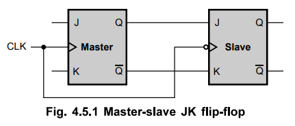
It consists of clocked JK flip-flop as a master and clocked JK flip-flop as a slave. The output of the master flip-flop is fed as an input to the slave flip-flop.
Master-Slave JK Flip-Flop
AU
: Dec.-05, 08, 10, 17, 18, May-05, 08, 15, 16, 17
•
Fig. 4.5.1 shows one way to build a JK master-slave flip-flop. It consists of
clocked JK flip-flop as a master and clocked JK flip-flop as a slave. The
output of the master flip-flop is fed as an input to the slave flip-flop. As
shown in the Fig. 4.5.1, clock signal is connected directly to the master
flip-flop, but it is connected through inverter to the slave flip-flop.
Therefore, the information present at the J and K inputs is transmitted to the
output of master flip-flop on the positive clock pulse and it is held there
until the negative clock pulse occurs, after which it is allowed to pass
through to the output of slave flip-flop.
•
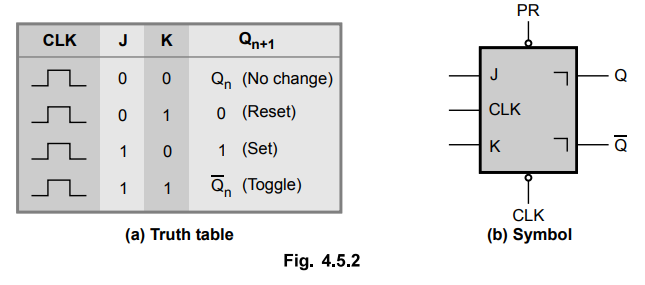
When J = 1 and K = 0, the master sets on the positive clock. The high Y output
of the master drives the J input of the slave, so at negative clock, slave
sets, copying the action of the master.
•
When J = 0 and K = 1, the master resets on the positive clock. The high ![]() output of the master goes
output of the master goes
to
the K input of the slave. Therefore, at the negative clock slave resets, again
copying the action of the master.
•
When J = 1 and K = 1, master toggles on the positive clock and slave then
copies the output of master on the negative clock.
•
When J = K = 0, the output of master remains same at the positive clock. Thus
the output of slave also remains same at the negative clock. The Fig. 4.5.2
shows the truth table and symbol for master-slave JK flip-flop.
Note
:
It is important to note that clock input of the master-slave flip-flop is not
edge triggered.
Review Questions
1. Explain the operation of JK master slave flip-flop with
suitable diagrams.
2. Describe the input and output action of JK master/slave
flip-flops.
3. Explain the working of a master-slave JK flip-flop.
4. Mention the major application of master slave flip-flop.
5. Describe the design procedure with neat diagram about 4 bit bidirectional shift register with parallel load.
Digital Logic Circuits: Unit III: (a) Flip-Flops : Tag: : Circuit diagram, Logic symbol, Truth table - Master-Slave JK Flip-Flop
Related Topics
Related Subjects

Digital Logic Circuits
EE3302 3rd Semester EEE Dept | 2021 Regulation | 3rd Semester EEE Dept 2021 Regulation